Digital Signal Processing
Digital signal processing encompasses methods for processing signals after converting them into digital form, such as radar processing. Radar systems basically generate pulses that can be fed through a directional antenna. These signals travel at the speed of light, and any object in their path reflects a small portion of the projected energy back to the radar receiving antenna. Calculating the difference between the transmitted and received signals tells you the distance and speed of the object.
DSPs are fundamental to radar systems and are used for a variety of functions such as pulse compression, signal filtering, and pulse modulation. Without DSPs, radar systems cannot accurately detect objects at long distances. DSPs differ from general-purpose microprocessors in that they are suited for the types of fast mathematical calculations (multiplication and addition) most commonly used when designing filters such as FFT and FIR. In general, FFT filters are used for domain conversion – from time domain to frequency domain or vice versa, while FIR filters are used for signal separation and recovery. These types of filters are commonly found in radar designs.
There are two main hardware approaches to implementing DSP: programmable DSP processors and field programmable gate arrays ( FPGAs ). In both approaches, the DSP architecture is well suited for DSP algorithms.
DSP Processor
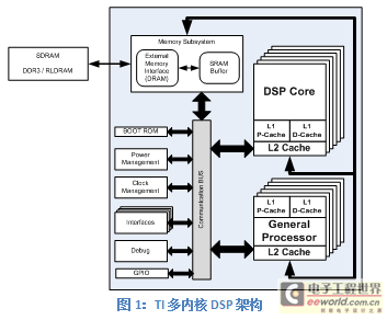
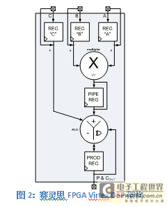
如图1所示的TI多内核DSP等DSP处理器采用专用硬件计算每个周期的乘法运算。现代DSP处理器的指令集允许编程人员在单个指令中指定多个并行运算,一般在主算术运算进行的同时一次或多次从存储器提取数据。另外,为了显著改善每个时钟周期的DSP性能,DSP架构目前包含并行运行的附加乘法器与加法器,从而可以在单个指令中编码并行运算。
DSP Memory Requirements
Executing DSP functions every cycle requires the ability to efficiently fetch instructions and data from memory. Therefore, the key to maintaining DSP performance is high memory bandwidth. DSP processors and FPGA DSP blocks have established internal cache memory architectures (L1/L2) to support multiple memory accesses per cycle. Using separate memory banks to store instructions and data, a super Harvard architecture can be implemented. With this arrangement, the processor can fetch instructions and data operands in parallel every cycle. In addition, memory accesses in DSP algorithms generally exhibit predictable patterns. For example, FIR filter coefficients are accessed in a sequential loop. For deeper external storage, a hardware-based external memory interface (EMIF) that supports various SDR AM memories (DDR2/3, RLDRAM) is generally used.
To achieve a two-fold increase in DSP performance, a new innovative approach to external storage using QDR SRAM can be implemented.
Quad Data Rate (QDR) Architecture
SRAMs such as the Cypress QDR-IV SRAM shown in Figure 3 are high-performance memory devices that are carefully optimized for high throughput. This type of memory has multiple independent data ports with a double data rate (DDR) interface. Access to these data ports can be simultaneous and independent of each other. The address bus is shared and operates at single or double data rates depending on the configuration. The highest density product on the market today is 144Mb, and supports 18x or 36x configurations.
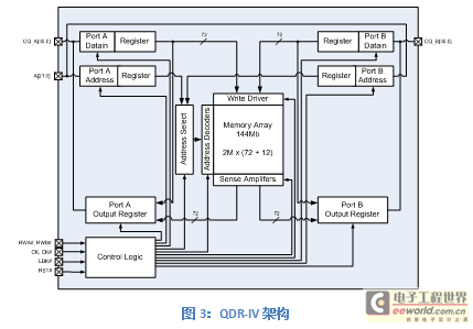
The architectural features of the QDR-IV SDR AM are highly advantageous for digital signal processing flows that require high throughput, low latency, and true random access.
Comparison between the traditional method ( SDR AM) and the new method (QDR-IV)
The overall setup of the test environment is illustrated in Figure 4. The highest data throughput of different memory types was compared using FPGA-based DSP functions.
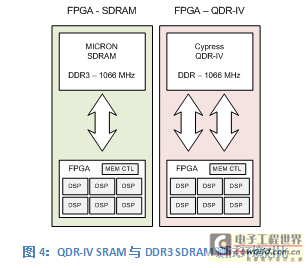
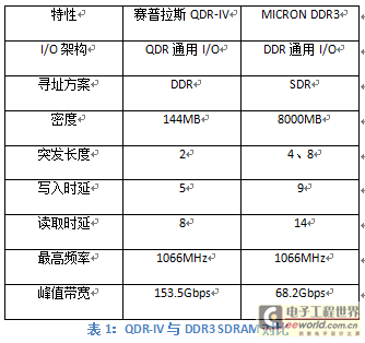
The following table compares the key performance parameters of QDR-IV SRAM and DDR3 SDR AM memory technologies.
Reference address of this article: http://www.eepw.com.cn/article/247534.htm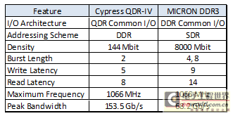
Table 1 shows that QDR-IV can provide more than twice the bandwidth of DDR3 SDR AM when running at the same frequency. In addition, the dual independent ports of QDR-IV SRAM generate output signals while acquiring input signals, which can easily meet the data requirements of the real-time processing functions of DSP . Therefore, the bottleneck problem of transferring data to and extracting data from the memory can be alleviated.
SAR radar perspective
SAR radars that observe the Earth’s surface at high resolution require transposed memory accesses, where the range and azimuth directions are transposed for reconstruction processing. Efficient FFT and IFFT ( DSP ) operations between range and azimuth compression processing can achieve this. The architectural advantages of QDR SRAM can improve the performance of SAR radars by achieving fast and consistent memory access times. Figure 5 illustrates the transposition problem associated with SAR image reconstruction:
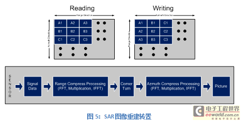
When using traditional SDR AM memory, writing SAR image data (as shown in the figure) results in a discontinuous address space, which reduces processor performance (estimated to be about 5 times in this case). Since QDR-IV's independent read and write ports support parallel operations and random memory access, the impact on processing power can be reduced.
QDR SRAM provides a high-performance alternative to traditional SDRAM for off-chip data storage in DSP -based applications. The density limitations of QDR SRAM can be eliminated by cascading multiple devices. This approach is ideal for applications that require higher random access throughput because faster memory access improves DSP performance.
Previous article:A 3G video helmet design based on ARM11 and DSP
Next article:A brief analysis of the development and relationship of the two major markets of DSP and FPGA
Recommended ReadingLatest update time:2024-11-22 20:19


- Popular Resources
- Popular amplifiers
- "Cross-chip" quantum entanglement helps build more powerful quantum computing capabilities
- Why is the vehicle operating system (Vehicle OS) becoming more and more important?
- Car Sensors - A detailed explanation of LiDAR
- Simple differences between automotive (ultrasonic, millimeter wave, laser) radars
- Comprehensive knowledge about automobile circuits
- Introduction of domestic automotive-grade bipolar latch Hall chip CHA44X
- Infineon Technologies and Magneti Marelli to Drive Regional Control Unit Innovation with AURIX™ TC4x MCU Family
- Power of E-band millimeter-wave radar
- Hardware design of power supply system for automobile controller
 Professor at Beihang University, dedicated to promoting microcontrollers and embedded systems for over 20 years.
- Intel promotes AI with multi-dimensional efforts in technology, application, and ecology
- ChinaJoy Qualcomm Snapdragon Theme Pavilion takes you to experience the new changes in digital entertainment in the 5G era
- Infineon's latest generation IGBT technology platform enables precise control of speed and position
- Two test methods for LED lighting life
- Don't Let Lightning Induced Surges Scare You
- Application of brushless motor controller ML4425/4426
- Easy identification of LED power supply quality
- World's first integrated photovoltaic solar system completed in Israel
- Sliding window mean filter for avr microcontroller AD conversion
- What does call mean in the detailed explanation of ABB robot programming instructions?
- 2024 China Automotive Charging and Battery Swapping Ecosystem Conference held in Taiyuan
- State-owned enterprises team up to invest in solid-state battery giant
- The evolution of electronic and electrical architecture is accelerating
- The first! National Automotive Chip Quality Inspection Center established
- BYD releases self-developed automotive chip using 4nm process, with a running score of up to 1.15 million
- GEODNET launches GEO-PULSE, a car GPS navigation device
- Should Chinese car companies develop their own high-computing chips?
- Infineon and Siemens combine embedded automotive software platform with microcontrollers to provide the necessary functions for next-generation SDVs
- Continental launches invisible biometric sensor display to monitor passengers' vital signs
- Another technical solution for power-type plug-in hybrid: A brief discussion on Volvo T8 plug-in hybrid technology
- Some interesting creative sharing
- Fresh graduates are joining the Greater Shanghai community to study for a master's degree in engineering at a prestigious university!
- [Evaluation of EC-01F-Kit, the NB-IoT development board of Anxinke] 05. Communication based on STM32+EC-01F Socket
- How to disassemble an integrated circuit
- The evaluation plan for the current probe and signal generator winners is open! The instruments have been distributed, and we look forward to the sharing of the 6 little ones
- Embedded Qt-Control Hardware: Slide bar controls RGB lights
- Technical Article: 24-bit Data Acquisition System for IEPE Sensors
- Corelink SinA33 development board virtual machine compiled source code
- Hardware Verification Language - Introduction
- 【Recruitment】RF Engineer

 FPGA implementation of FIR filter
 Analysis and Implementation of MAC Protocol for Wireless Sensor Networks (by Yang Zhijun, Xie Xianjie, and Ding Hongwei)


 京公网安备 11010802033920号