1. Overview: In recent years, with the rapid development of digital signal processing technology and the continuous emergence of new theories and algorithms, coupled with the overall improvement in the performance of digital signal processing devices, actual systems have increasingly higher requirements for analog-to-digital converters. . Therefore, in practical applications, analog-to-digital converters are generally required to have both a high sampling rate and accuracy, a large dynamic range, an extremely wide frequency response range, and a flexible digital interface.
2. ADS5500 is a high-performance analog-to-digital converter with 14-bit resolution and 125MSPS sampling rate developed by Texas Instruments. The chip is packaged in a 64-pin TQFP PowerPAD. To achieve higher system integration, it also includes a complete conversion solution with wide-bandwidth linear sample/hold and internal reference voltage source. The ADS5500 has a signal-to-noise ratio (SNR) of 70dB, a distortion-free dynamic range (SFDR) of 82dB at 100MHz, a differential input voltage of 2.2Vpp, an operating voltage of 3.3V (unipolar), and a power consumption of only 750mW. The internal reference voltage simplifies system design, and the parallel CMOS-compatible data output interface ensures seamless connection with ordinary logic circuits and facilitates connection with digital signal processors (DSPs). The chip operating temperature is -40oC to +85oC.
Based on its high sampling rate, high resolution, and simple interface, the ADS5500 can be widely used in situations that require high-speed data sampling and high-precision measurement, such as wireless communications, communication receivers, base station infrastructure equipment, test and measurement instruments, single and multiple channel digital receivers, communication instruments, radar and infrared technology, video image processing, and medical equipment.


3 Design considerations
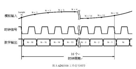
The ADS5500 is a 14-bit pipeline analog-to-digital converter with low power consumption and a sampling rate of 125MSPS. It only needs a 3.3V unipolar power supply to operate normally. The data conversion process starts on the rising edge of the clock signal waveform. Once the analog signal is captured by the sample/hold part of the converter, the sampling process of the input signal is sequentially divided into a series of pipeline operations, so that the rising edge and falling edge of the clock signal Data conversion can be performed along all directions. A delay of 16 clock cycles is required from inputting an analog signal to outputting 14-bit data. Figure 2 shows the corresponding timing of the ADS5500 input, output signals and clock waveforms.

3.1 Input configuration
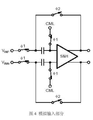
The analog input part of the ADS5500 mainly consists of a differential track/hold amplifier and switched capacitors, as shown in Figure 4.

Differential input technology ensures high performance at high sampling rates and also brings very high usable input bandwidth, which is especially important for certain intermediate frequency sampling or undersampling applications. For the input configuration of low-frequency input signals, a differential input/output amplifier (such as OPA695) can be used to simplify the front-end drive circuit. The advantage of this configuration is that it has greater flexibility. The amplifier can be used to complete the polarity conversion (unipolar to differential) of the analog input signal, signal amplification, and front-end pre-filtering of the ADC.
3.2 Reference source circuit
The internal voltage reference of the ADS5500 simplifies the circuit layout of the circuit board, and no additional circuitry is required on the board. However, from the perspective of optimizing performance, a 1μF capacitor can be connected to the REFP and REFM pins each and connected to ground. In addition, in order to better set the working current of the chip, a 47Ω resistor should be connected to the IREF pin and connected to the AGND pin, as shown in Figure 5.

3.3 Clock input signal
The clock input signal of the chip can be a unipolar or differential signal. In normal mode, the voltage amplitude of the clock input signal is set to 1.5V. The CLKP pin and CLKM pin are each connected to the CM pin through a 5kΩ resistor, as shown in Figure 7 shown.

From a practical perspective, selecting a low-jitter clock source and performing corresponding band-pass filtering can greatly improve the performance of high-frequency sampling systems. The ADC core inside the chip can perform data conversion on both the rising and falling edges of the clock signal waveform, further improving the chip's working efficiency. When there is no clock source or the clock frequency is lower than 10MSPS, the chip will automatically switch to sleep mode.
3.4 Output options
The chip generates a 14-bit data output signal (D13┄D0, where D13 is the highest bit and D0 is the lowest bit), 1 data ready signal (CLKOUT pin) and 1 data overflow indication bit (OVR pin, when outputting data When the amplitude exceeds the maximum value, this bit is set to 1).
The data format of the output signal and the polarity of the clock output signal can be set by changing the DFS pin level. The data format of the output signal has two forms: direct binary code and two's complement, and the clock polarity shows that the output data is valid on the rising edge or falling edge of the clock waveform. There are four selection ranges for the DFS pin level, so there are four corresponding relationships. Table 2 gives the correspondence between these four modes.
Table 2 Selection of output data format and clock signal polarity

3.5 Application examples
The following is a real-time image processing system. The CCD sensor sends the original image (analog signal) to the ADS5500 high-frequency sampling to obtain a high-precision digital image signal, which is then sent to the image processing unit through the high-speed synchronous FIFO. The digital signal processor Complete image processing and compression, and display the processed data on an LCD or CRT monitor.

Conclusion
The ADS5500 has a simple interface, is easy to use and flexible, has 14-bit sampling accuracy, and has a high conversion speed. This chip is highly practical in most applications that require high-speed data acquisition and high-precision measurement.
references
1. Texas Instruments. ADS5500: 14-Bit, 125MSPS Analog-to-Digital Converter. 2003: 8~12.
2. Texas Instruments. Video and Imaging Solutions Guide. 2002:4~8.
3.Tan Jie Hoffner. Dynamic parameters of high-speed A/D converters [J]. Electrical Measurement and Instrumentation, 2001; 38(3): 31~33.
4. Ruan Qiuqi. Digital Image Processing[M]. Beijing: Electronic Industry Press, 2001: 213~218.
Previous article:High-side current sensor AD8205 and its applications
Next article:14-bit 125Msps analog-to-digital converter ADS5500 and its applications
Recommended ReadingLatest update time:2024-11-16 19:57


- High signal-to-noise ratio MEMS microphone drives artificial intelligence interaction
- Advantages of using a differential-to-single-ended RF amplifier in a transmit signal chain design
- ON Semiconductor CEO Appears at Munich Electronica Show and Launches Treo Platform
- ON Semiconductor Launches Industry-Leading Analog and Mixed-Signal Platform
- Analog Devices ADAQ7767-1 μModule DAQ Solution for Rapid Development of Precision Data Acquisition Systems Now Available at Mouser
- Domestic high-precision, high-speed ADC chips are on the rise
- Microcontrollers that combine Hi-Fi, intelligence and USB multi-channel features – ushering in a new era of digital audio
- Using capacitive PGA, Naxin Micro launches high-precision multi-channel 24/16-bit Δ-Σ ADC
- Fully Differential Amplifier Provides High Voltage, Low Noise Signals for Precision Data Acquisition Signal Chain
- Innolux's intelligent steer-by-wire solution makes cars smarter and safer
- 8051 MCU - Parity Check
- How to efficiently balance the sensitivity of tactile sensing interfaces
- What should I do if the servo motor shakes? What causes the servo motor to shake quickly?
- 【Brushless Motor】Analysis of three-phase BLDC motor and sharing of two popular development boards
- Midea Industrial Technology's subsidiaries Clou Electronics and Hekang New Energy jointly appeared at the Munich Battery Energy Storage Exhibition and Solar Energy Exhibition
- Guoxin Sichen | Application of ferroelectric memory PB85RS2MC in power battery management, with a capacity of 2M
- Analysis of common faults of frequency converter
- In a head-on competition with Qualcomm, what kind of cockpit products has Intel come up with?
- Dalian Rongke's all-vanadium liquid flow battery energy storage equipment industrialization project has entered the sprint stage before production
- Allegro MicroSystems Introduces Advanced Magnetic and Inductive Position Sensing Solutions at Electronica 2024
- Car key in the left hand, liveness detection radar in the right hand, UWB is imperative for cars!
- After a decade of rapid development, domestic CIS has entered the market
- Aegis Dagger Battery + Thor EM-i Super Hybrid, Geely New Energy has thrown out two "king bombs"
- A brief discussion on functional safety - fault, error, and failure
- In the smart car 2.0 cycle, these core industry chains are facing major opportunities!
- The United States and Japan are developing new batteries. CATL faces challenges? How should China's new energy battery industry respond?
- Murata launches high-precision 6-axis inertial sensor for automobiles
- Ford patents pre-charge alarm to help save costs and respond to emergencies
- New real-time microcontroller system from Texas Instruments enables smarter processing in automotive and industrial applications
- Showing goods + NVIDIA AI small board
- Circuit diagram of two-wheeled electric vehicle
- [Domestic RISC-V Linux Board Fang·Starlight VisionFive Trial Report] Python output HELLOWORLD
- Solutions for control loop design
- Data size transferred after power failure
- About DMX dimming system
- What is UWB?
- Solution to blind area communication of intercom
- Xunwei i.MX8MM Development Board Linux Android 9.0 Crotex-M4 Data Update
- Commonly used algorithms for drones - Kalman filter (Part 3)

 Siemens PLC from Beginner to Mastery with Color Illustrations (Yang Rui)
 【Follow me Season 2 Episode 2】Arduion UR4 homework submission code


 京公网安备 11010802033920号