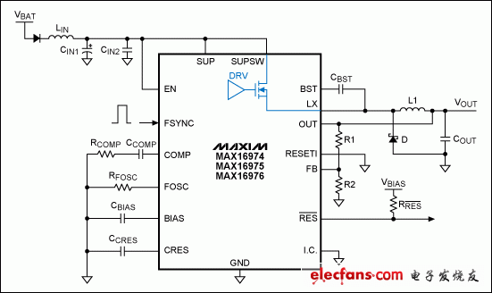
The MAX16974/MAX16975/MAX16976 converters are standard buck controllers designed for automotive applications. These controllers operate through an internal high-side N-channel field-effect transistor FET and an external freewheeling diode. Proper PCB (printed circuit board) layout, combined with appropriate external components, is essential for reliable system operation and minimizing EMI emissions. The circuit shown in Figure 1 shows a typical application circuit for these high-performance converters.
Typical application circuit

Figure 1. Typical application circuit
DC and AC current paths
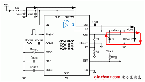
Figure 2 shows the AC and DC current paths for the MAX16974/MAX16975/MAX16976 family.

Figure 2a. DC current path when the HSFET is on (black) or the freewheeling diode is on (red).

Figure 2b. The AC branch of the DC current path shown in Figure 2a.
Effect of component position on AC current path
To optimize the board layout and reduce EMI, the AC current path in Figure 2b is critical. This path consists of input capacitors CIN1 and CIN2 and Schottky freewheeling diode D. The input capacitors maintain the IC input voltage stable at the SUB and SUBSW pins. CIN1 is a bulk capacitor, while CIN2 is a ceramic capacitor that generates transient currents. The location of CIN2 is critical and needs to be as close to the SUPSW and SUP pins as possible. Use two different capacitors as CIN2 and place them close to the SUPSW and SUP pins. If CIN2 is far away from SUP and SUPSW, the inductance between CIN2 and the IC pins will cause changes in the IC pin voltage, which directly affects the device performance.
The Schottky freewheeling diode is another important component that must be placed close to the LX pin of the IC. The LX pin is a switching pin, and when the DC current path switches between the "black" and "red" channels in Figure 2a, the current at this pin will also change transiently, forming a noise source for the IC. Placing the Schottky freewheeling diode close to the LX pin can keep the parasitic inductance as low as possible, which helps reduce the voltage change on the LX pin when the DC loop switches.
In addition, an RC network snubber can be placed as close as possible to the LX pin. The RC network helps suppress EMI and prevent voltage transients caused by distributed inductance. Another way to control the LX pin voltage is to connect a resistor in series with the bootstrap capacitor CBST. This will slow down the turn-on of the high-side field effect tube HSFET inside the IC, which in turn will limit the rise rate of the LX pin voltage.
Finally, the AC current loop formed by CIN2, HSFET, Schottky freewheeling diode and GND needs to be laid out as compactly as possible to reduce the loop area, so that the current flows in a smaller range and away from sensitive IC control pins.
Other component placement
After completing the layout of the above key components, the remaining components should be placed around. Inductor L1 and output capacitor COUT should be placed close to the device, and the corresponding DC loop should be as small as possible.
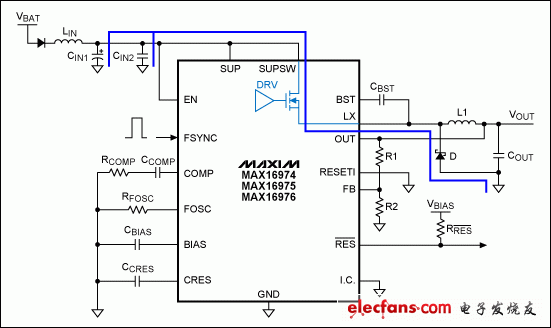
Another important component is the BIAS capacitor CBIAS, which is used to power all control circuits inside the IC. In addition, when the Schottky freewheeling diode is on during each switching cycle, the bootstrap capacitor CBST is charged through the bias capacitor, as shown in Figure 3.

Figure 3. Bootstrap capacitor charging path (green)
To ensure the BIAS pin operating voltage is stable, the capacitor CBIAS needs to be placed close to the IC pin to minimize the lead inductance between the BIAS pin and the capacitor CBIAS.
Thermal Considerations
The MAX16974 has an exposed pad on the bottom of the IC, which is the main heat dissipation channel of the device. The MAX16974 integrates a high-side field effect transistor HSFET inside, which can provide 2A drive. In order to obtain the maximum power from the device, proper soldering between the exposed pad and the PCB is critical. The exposed pad of the MAX16974 is at ground potential. Soldering it to the ground plane helps to dissipate the heat inside the package. The copper area needs to be added with vias and connected to the ground plane of other layers. These vias help improve the ground path and spread the heat inside the package to the PCB.
MAX16974 EV Kit Layout
Figures 4 to 8 show the schematic and layout of the MAX16974 evaluation kit (MAX16974EVKIT). The EV kit uses a 4-layer printed circuit board and follows the above layout guidelines. The inner two layers (Figures 6 and 7) are used as ground planes to help the MAX16974 dissipate heat through the exposed pad. These ground planes are mainly connected to the top layer exposed pad through vias.

Figure 4. MAX16974EVKIT schematic.

Figure 5. Top layer of the MAX16974 EV kit.

Figure 6. Layer 2 (ground plane) of the MAX16974 EV kit.

Figure 7. Layer 3 (ground) of the MAX16974 EV kit.

Figure 8. Bottom side of the MAX16974 EV kit.
Previous article:DisplayPort-based solution for multi-screen display
Next article:Introduction of LCD TV Panel
- Popular Resources
- Popular amplifiers
- High signal-to-noise ratio MEMS microphone drives artificial intelligence interaction
- Advantages of using a differential-to-single-ended RF amplifier in a transmit signal chain design
- ON Semiconductor CEO Appears at Munich Electronica Show and Launches Treo Platform
- ON Semiconductor Launches Industry-Leading Analog and Mixed-Signal Platform
- Analog Devices ADAQ7767-1 μModule DAQ Solution for Rapid Development of Precision Data Acquisition Systems Now Available at Mouser
- Domestic high-precision, high-speed ADC chips are on the rise
- Microcontrollers that combine Hi-Fi, intelligence and USB multi-channel features – ushering in a new era of digital audio
- Using capacitive PGA, Naxin Micro launches high-precision multi-channel 24/16-bit Δ-Σ ADC
- Fully Differential Amplifier Provides High Voltage, Low Noise Signals for Precision Data Acquisition Signal Chain
- LED chemical incompatibility test to see which chemicals LEDs can be used with
- Application of ARM9 hardware coprocessor on WinCE embedded motherboard
- What are the key points for selecting rotor flowmeter?
- LM317 high power charger circuit
- A brief analysis of Embest's application and development of embedded medical devices
- Single-phase RC protection circuit
- stm32 PVD programmable voltage monitor
- Introduction and measurement of edge trigger and level trigger of 51 single chip microcomputer
- Improved design of Linux system software shell protection technology
- What to do if the ABB robot protection device stops
- Ranking of installed capacity of smart driving suppliers from January to September 2024: Rise of independent manufacturers and strong growth of LiDAR market
- Industry first! Xiaopeng announces P7 car chip crowdfunding is completed: upgraded to Snapdragon 8295, fluency doubled
- P22-009_Butterfly E3106 Cord Board Solution
- Keysight Technologies Helps Samsung Electronics Successfully Validate FiRa® 2.0 Safe Distance Measurement Test Case
- Innovation is not limited to Meizhi, Welling will appear at the 2024 China Home Appliance Technology Conference
- Innovation is not limited to Meizhi, Welling will appear at the 2024 China Home Appliance Technology Conference
- Huawei's Strategic Department Director Gai Gang: The cumulative installed base of open source Euler operating system exceeds 10 million sets
- Download from the Internet--ARM Getting Started Notes
- Learn ARM development(22)
- Learn ARM development(21)
- Thermal fatigue analysis of power modules
- FOC sensorless motor control video
- Design of embedded network interface controller based on FPGA
- SHT31 Review Summary
- The differential voltage measured by the oscilloscope when the RS485 bus is idle is ±3.7V, and the periodic waveform with a frequency of 50hz
- What are the functions of magnetic beads and capacitors? How to choose the impedance of magnetic beads and the size of capacitors?
- Why would the filter added to the final stage cavity be burned?
- 【Beetle ESP32-C3】GNSS test
- Arteli AT32 uses GPIO to simulate HDMI CEC case
- Analyze the cause of tms320c6455 burning

 CMOS_Transistor_Layout_KungFu


 京公网安备 11010802033920号