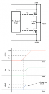
Figure 1. Simplified output stage and power-on glitch.
Previously, the causes of power-on/off glitches on the buffered outputs of precision DACs and solutions to reduce these glitches have been analyzed. This brief focuses on the power-on glitch that occurs when the DAC output buffer is powered up in voltage output mode. A precision DAC can be powered up in multiple configurations: zero scale, mid-scale, or high impedance. The user can control the pre-power-off state. Some DACs have built-in power-on glitch reduction (POGR) circuitry; this circuit maintains the DAC output stage in a configuration where the DAC output stage is not driven. Buffered voltage output DACs have a pair of PFETs and NFETs as the output stage. The POGR circuit disables the PFET and biases the NFET above its threshold voltage (VTH), thereby minimizing the power-on glitch to a few hundred millivolts.
Not every DAC has a POGR circuit in it. For DACs without POGR, the power-on/off glitch pulse depends on several factors:
1. The power-on state of the DAC to voltage output mode and high impedance mode
2. The power-on sequence of DVDD, VREF, IOVDD and other power pins
3. Feedback network connection
4. Power supply ramp rate
5. Output resistive load
This article discusses the case where the output stage is powered up in voltage output mode. In this mode, the gates of the PFET and NFET are controlled by a pre-output stage. This pre-output stage requires a certain minimum voltage to start up properly. This voltage is also called the minimum headroom (VH). This voltage depends on the pre-output stage architecture and can be as high as 6V. This voltage is much lower than the minimum supply voltage (VDDMIN) specified in the datasheet. Typically, this voltage is not specified in most datasheets.
Before this minimum headroom voltage is reached, the pre-output stage does not have enough headroom for normal operation. Therefore, the output FET gate can go as low as 0V, which allows the PFET to operate as a low-resistance switch between the supply and the output pin when the supply voltage crosses the PFET threshold voltage (VTP). As a result, the output is able to ramp up with the supply, resulting in a power-on glitch (see Figure 1).
In this case, the glitch voltage can be as high as the minimum headroom voltage (VH). This glitch is independent of the supply ramp rate due to insufficient headroom in the pre-output stage. All DAC datasheets specify a minimum resistive load on the output (usually 1kW). Adding a resistive load to the DAC output is a common technique to minimize this glitch. However, this technique does not minimize the glitch amplitude because the output PFET operates as a switch (or short) between the supply and the output pin. The power-up sequence and feedback network connections can further increase this glitch. Because these factors are often interrelated, they are analyzed as one case.

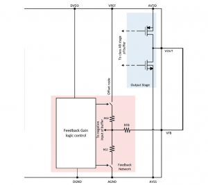
Figure 2. Output stage with feedback network.
For dual-supply DACs with bipolar outputs, the feedback network also includes an offset node. This node can be driven by a fixed voltage (VREF) on the reference pin or by an offset DAC. An offset DAC is useful when the user needs a small voltage offset output to achieve an asymmetrical output range; for example, from -5V to +10V.
Figure 2 is a simplified diagram of an output stage with a feedback network. This feedback network requires switches to change the gain and offset of the DAC. These switches have a separate digital supply, or DVDD supply. Depending on the DVDD power-up sequence, the gain/offset path will be open or shorted to the VREF/AGND pin. This will result in an incorrect gain setting during startup and a power-up glitch. In most multi-supply DACs, a specific power-up sequence is recommended to avoid this.
The power-on glitch pulse is independent of the state of the DAC registers. When the DAC is powered up with a circuit called the power-on reset (POR), all DAC registers are held in a reset state. When these registers are released from the reset state after a period of time, the output and pre-output stage have enough headroom to operate normally.

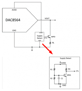
Figure 3. Simple power detection circuit
A simple power detection circuit (Figure 3) can be used to load the DAC output immediately during the power ramp. The DAC output VOUT is loaded with resistor RL through FET MPD during the power ramp. This power detection block generates the MPD control. During the power ramp, the control signal CTL is pulled to AVDD, loading the DAC output VOUT with load RL before FET MN1 is turned on. After MN1 is fully turned on, it pulls the CTL node to ground, unloading the VOUT node. R1, R2, R3, and CL must be sized according to the threshold voltage of MN1.
This article analyzes the power-on glitch and its root causes. Although the analysis is focused on solving the power-on glitch, the same principles apply to the power-off glitch. A small resistive load between the output pin and ground during startup is the only way to minimize the power-on glitch for certain DACs that are powered up in normal mode without an internal POGR circuit.
Previous article:Extreme environments drive design innovation
Next article:How to reduce power-on/off glitches in high-precision DACs
- Popular Resources
- Popular amplifiers
- High signal-to-noise ratio MEMS microphone drives artificial intelligence interaction
- Advantages of using a differential-to-single-ended RF amplifier in a transmit signal chain design
- ON Semiconductor CEO Appears at Munich Electronica Show and Launches Treo Platform
- ON Semiconductor Launches Industry-Leading Analog and Mixed-Signal Platform
- Analog Devices ADAQ7767-1 μModule DAQ Solution for Rapid Development of Precision Data Acquisition Systems Now Available at Mouser
- Domestic high-precision, high-speed ADC chips are on the rise
- Microcontrollers that combine Hi-Fi, intelligence and USB multi-channel features – ushering in a new era of digital audio
- Using capacitive PGA, Naxin Micro launches high-precision multi-channel 24/16-bit Δ-Σ ADC
- Fully Differential Amplifier Provides High Voltage, Low Noise Signals for Precision Data Acquisition Signal Chain
- LED chemical incompatibility test to see which chemicals LEDs can be used with
- Application of ARM9 hardware coprocessor on WinCE embedded motherboard
- What are the key points for selecting rotor flowmeter?
- LM317 high power charger circuit
- A brief analysis of Embest's application and development of embedded medical devices
- Single-phase RC protection circuit
- stm32 PVD programmable voltage monitor
- Introduction and measurement of edge trigger and level trigger of 51 single chip microcomputer
- Improved design of Linux system software shell protection technology
- What to do if the ABB robot protection device stops
- Allegro MicroSystems Introduces Advanced Magnetic and Inductive Position Sensing Solutions at Electronica 2024
- Car key in the left hand, liveness detection radar in the right hand, UWB is imperative for cars!
- After a decade of rapid development, domestic CIS has entered the market
- Aegis Dagger Battery + Thor EM-i Super Hybrid, Geely New Energy has thrown out two "king bombs"
- A brief discussion on functional safety - fault, error, and failure
- In the smart car 2.0 cycle, these core industry chains are facing major opportunities!
- The United States and Japan are developing new batteries. CATL faces challenges? How should China's new energy battery industry respond?
- Murata launches high-precision 6-axis inertial sensor for automobiles
- Ford patents pre-charge alarm to help save costs and respond to emergencies
- New real-time microcontroller system from Texas Instruments enables smarter processing in automotive and industrial applications
- Share an easy-to-understand msp430 microcontroller learning tutorial
- Simulation of a Microstrip Patch Antenna for 2.4 GHz Applications with Radiat...
- Shenzhen is so beautiful
- New mpy board
- EEWORLD University Hall----FPGA Design Skills and Specifications
- C8051F040 has a CAN interrupt, how to determine which mailbox caused the interrupt
- [RISC-V MCU CH32V103 Review] + EXTI interrupt input switch OLED
- TinyGo, the GO language for microcontrollers
- Design and implementation of multiple image fusion and superposition based on FPGA (1)
- Development of FPGA Industry

 BA3129FE2


 京公网安备 11010802033920号