In the Matlab/Simulink environment, the DSP Builder module was used to build the FIR model, and the FIR filter was designed according to the FDATool tool. Then, system-level simulation and ModelSim functional simulation were performed. The simulation results show that the filtering effect of the digital filter is good. The model was converted into VHDL language through SignalCompiler and added to the hardware design of FPGA. The real-time result waveform of the digital filter was obtained from the virtual logic analysis tool SignalTapⅡ in QuartusⅡ software, and the result was in line with expectations.
0 Introduction
In the process of information signal processing, digital filter is the most widely used method in signal processing. Through filtering operation, a set of input data sequence is transformed into another set of output data sequence, thereby realizing the change of signal properties in time domain or frequency domain. Commonly used digital filters can be divided into two types: finite impulse response (FIR) filter and infinite impulse response (IIR) filter. Among them, FIR digital filter has a strict linear phase, and the non-recursive structure also ensures the stability of operation. In applications with high real-time requirements, programmable chip FPGA is used for implementation. Compared with the implementation method of DSP chip or dedicated chip, it has the advantages of high speed, high precision and high flexibility. This paper adopts a method based on FPGA and DSP Builder to design FIR digital filter, adopts hierarchical and modular design ideas, follows the design and development process of DSP Builder, establishes a model in Matlab/Simulink and performs system-level simulation, and then performs Verilog language conversion. After ModelSim simulation verification, the real-time test of FIR digital filter is realized.
1 Basic principles and structure of FIR digital filter
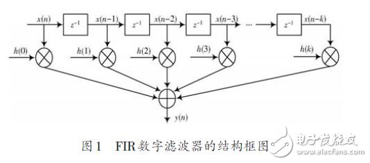
For a FIR filter system, its impulse response is always finite, and its system function can be written as:

Where: x(n) is the input sampling sequence; h(i) is the filter coefficient; k is the filter order; y(n) represents the output sequence of the filter.
Figure 1 is a structural block diagram of a k-order FIR digital filter.

2 FIR digital filter design process
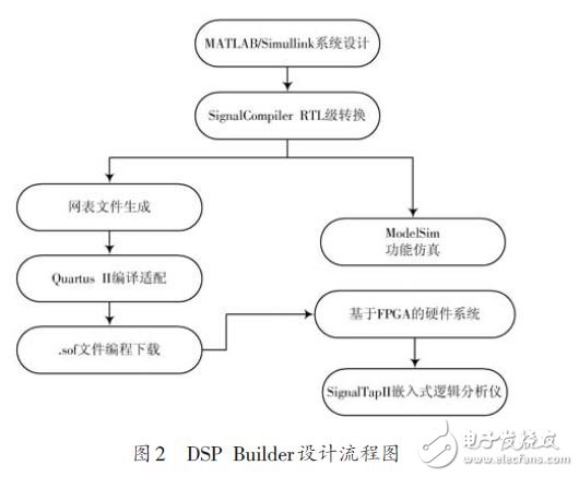
The design process mainly involves the development and design of tool software such as Matlab/Simulink, DSPBuilder and Quartus II. The entire design process, including system description to hardware implementation, can be completed in a complete design environment, as shown in Figure 2.

(1) Design input in Matlab/Simulink, that is, create a model file with the extension mdl in the Simulink environment of Matlab, and call the graphical modules (Block) in Altera DSP Builder and other Simulink libraries in a graphical way to form a system-level or algorithm-level design block diagram (or Simulink design model).
(2) Use Simulink's graphical simulation and analysis functions to analyze the correctness of the design model and complete model simulation, also called system-level simulation.
(3) A key step in DSP Builder design implementation is to convert Simulink model files into Verilog files, a universal hardware description language, through Signal-Compiler.
(4) The converted Verilog source code is functionally simulated using ModelSim software to verify the correctness of the Verilog file. The next few steps are to synthesize, compile and adapt the Verilog RTL code and simulation files generated by the above design in Quartus II tool software, generate a file with the extension .sof and load it into the FPGA hardware system.
3 Detailed Design of FIR Digital Filter
3.1 FIR digital filter module design and system-level simulation
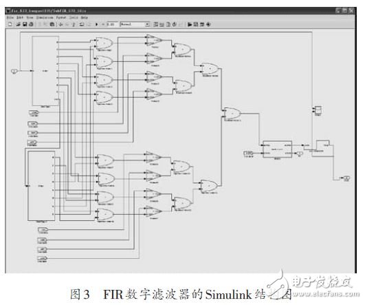
According to the principle of FIR digital filter, a 16-order FIR digital filter structure is built in the Simulink environment, as shown in Figure 3.
In the process of building the model, two 8-bit Shift Taps shift register modules were used to decompose the input signal, and then the algorithm calculation was performed according to the principle of digital filter.

Previous article:Design of high-definition digital video display interface based on DM6446 (Part 2)
Next article:Design of FIR digital filter based on FPGA (Part 2)
Recommended ReadingLatest update time:2024-11-16 15:55


- Popular Resources
- Popular amplifiers
-
 Analysis and Implementation of MAC Protocol for Wireless Sensor Networks (by Yang Zhijun, Xie Xianjie, and Ding Hongwei)
 -
 MATLAB and FPGA implementation of wireless communication
 -
 Intelligent computing systems (Chen Yunji, Li Ling, Li Wei, Guo Qi, Du Zidong)
 -
 Summary of non-synthesizable statements in FPGA
- High signal-to-noise ratio MEMS microphone drives artificial intelligence interaction
- Advantages of using a differential-to-single-ended RF amplifier in a transmit signal chain design
- ON Semiconductor CEO Appears at Munich Electronica Show and Launches Treo Platform
- ON Semiconductor Launches Industry-Leading Analog and Mixed-Signal Platform
- Analog Devices ADAQ7767-1 μModule DAQ Solution for Rapid Development of Precision Data Acquisition Systems Now Available at Mouser
- Domestic high-precision, high-speed ADC chips are on the rise
- Microcontrollers that combine Hi-Fi, intelligence and USB multi-channel features – ushering in a new era of digital audio
- Using capacitive PGA, Naxin Micro launches high-precision multi-channel 24/16-bit Δ-Σ ADC
- Fully Differential Amplifier Provides High Voltage, Low Noise Signals for Precision Data Acquisition Signal Chain
- Innolux's intelligent steer-by-wire solution makes cars smarter and safer
- 8051 MCU - Parity Check
- How to efficiently balance the sensitivity of tactile sensing interfaces
- What should I do if the servo motor shakes? What causes the servo motor to shake quickly?
- 【Brushless Motor】Analysis of three-phase BLDC motor and sharing of two popular development boards
- Midea Industrial Technology's subsidiaries Clou Electronics and Hekang New Energy jointly appeared at the Munich Battery Energy Storage Exhibition and Solar Energy Exhibition
- Guoxin Sichen | Application of ferroelectric memory PB85RS2MC in power battery management, with a capacity of 2M
- Analysis of common faults of frequency converter
- In a head-on competition with Qualcomm, what kind of cockpit products has Intel come up with?
- Dalian Rongke's all-vanadium liquid flow battery energy storage equipment industrialization project has entered the sprint stage before production
- Allegro MicroSystems Introduces Advanced Magnetic and Inductive Position Sensing Solutions at Electronica 2024
- Car key in the left hand, liveness detection radar in the right hand, UWB is imperative for cars!
- After a decade of rapid development, domestic CIS has entered the market
- Aegis Dagger Battery + Thor EM-i Super Hybrid, Geely New Energy has thrown out two "king bombs"
- A brief discussion on functional safety - fault, error, and failure
- In the smart car 2.0 cycle, these core industry chains are facing major opportunities!
- The United States and Japan are developing new batteries. CATL faces challenges? How should China's new energy battery industry respond?
- Murata launches high-precision 6-axis inertial sensor for automobiles
- Ford patents pre-charge alarm to help save costs and respond to emergencies
- New real-time microcontroller system from Texas Instruments enables smarter processing in automotive and industrial applications
- Award-winning live broadcast: ADI's technology and product registration for China's energy Internet applications has begun~
- Speechless! There will be a noise bump in the spectrum when there is no signal input at low frequency. Can you experts see what's going on?
- AD ground line width setting
- Is this injury serious?
- EEWORLD University Hall----Start using UCD3138 digital power controller tool
- CircuitPython 5.3.0-rc.0 released
- TI DSP programming - TMS320C6416
- CCS Error
- Packaging form and packaging process of RFID electronic tags
- Robot? Toy? Toy robot?

 Analysis and Implementation of MAC Protocol for Wireless Sensor Networks (by Yang Zhijun, Xie Xianjie, and Ding Hongwei)


 京公网安备 11010802033920号