The development of ARINC429 bus interface board realizes the reception and transmission of multi-channel ARINC429 bus data, which has become the focus of the current research on aircraft airborne bus interface.
1 ARINC429 Bus Introduction
In modern civil aircraft, a large amount of information needs to be transmitted between systems and between systems and components. The ARINC specification is an industrial standard for aviation transportation developed to transmit digital data information between avionics equipment.
The ARINC429 (hereinafter referred to as 429) bus protocol was proposed by the U.S. Aviation Electronics Engineering Committee in July 1977, and was published and approved for use in the same year. Its full name is Digital Information Transmission System DITS. The protocol standard specifies the requirements for digital information transmission between avionics equipment and related systems. ARINC429 is widely used in advanced civil airliners, such as B-737, B-757, and B-767. Russian military aircraft also use similar technology. Our corresponding standard is HB6096-SZ-01. The ARINC429 bus has a simple structure, stable performance, and strong anti-interference. The biggest advantage is high reliability, which is due to decentralized control, reliable transmission, and good error isolation.
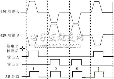
The 429 bus uses twisted shielded wires to transmit information, and transmits inversely through a pair of twisted wires, which has strong anti-interference capabilities. The modulation method uses a three-state code method of bipolar return to zero, that is, the information is modulated by a three-level state consisting of "high", "zero" and "low" states. The signal on the 429 cable and the signal after level conversion are shown in Figure 1. Each word of the 429 bus is 32 bits, and its word synchronization is based on a time interval of at least 4 bits of the transmission cycle, that is, a 4-bit code word.

Figure 1 429 signal and waveform after level conversion
2 System Overall Plan
The main function of the 429 bus interface board is to act as a bridge between the 429 signal and related peripherals. It can receive the bipolar return-to-zero 429 signal and convert it into a digital signal to send to the computer or other devices, and it can also convert the digital signal sent by the computer or other devices into a 429 signal output. The bus interface board introduced in this article uses FPGA and DSP to implement four 429 signal receiving channels and four 429 signal sending channels, and each channel is independent of each other. In this interface board, the time interval between every two data words is adjustable, each transceiver channel can define the word interval length separately, each channel check mode can be defined separately as odd check or even check, and data transmission can choose single frame transmission or automatic repeated transmission (repeated transmission of a certain frame).
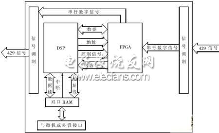
The entire interface board consists of a modulation circuit, a demodulation circuit, an FPGA, a DSP, and a dual-port RAM, as shown in Figure 2.

Figure 2 Interface board hardware structure diagram
3 Hardware Circuit Design
3.1 Modulation and demodulation circuit design
After the 429 signal enters the interface board, it must first be converted into a TTL level that can be recognized by the digital circuit. Here, HOLT's HI-8482 is used to demodulate the signal and convert the standard 429 bus signal into a 5V TTL digital signal. In order to reduce interference, 39pF high-precision military capacitors are connected to the four input pins of the 429 bus signal; HOLT's HI-8585 chip is used to modulate the signal and convert the TTL digital level into a standard 429 signal.
3.2 FPGA internal logic design
According to the coding format, characteristics, transmission rules and protocol requirements of the 429 signal, an ACEX1K FPGA from ALTERA is selected to send and receive four channels of data. Each channel is divided into a receiving part and a sending part.
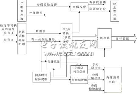
The main function of the receiving part is to convert serial data into 32-bit parallel data through serial/parallel conversion, and automatically perform error control on the received data. It can automatically detect errors such as word spacing and bit spacing errors. If there are no errors, the data will be sent to the DSP's 16-bit data bus twice for reading. The receiving module structure block diagram is shown in Figure 3.

Figure 3 Receiver module structure diagram
Previous article:Analysis of automotive TPMS sensor technology
Next article:Research on DSP+FPGA Airborne Bus Interface Board (Part 2)
Recommended ReadingLatest update time:2024-11-17 06:50


- Popular Resources
- Popular amplifiers
-
 Analysis and Implementation of MAC Protocol for Wireless Sensor Networks (by Yang Zhijun, Xie Xianjie, and Ding Hongwei)
 -
 MATLAB and FPGA implementation of wireless communication
 -
 Modern arc welding power supply and its control
 -
 Intelligent Control Technology of Permanent Magnet Synchronous Motor (Written by Wang Jun)
- High signal-to-noise ratio MEMS microphone drives artificial intelligence interaction
- Advantages of using a differential-to-single-ended RF amplifier in a transmit signal chain design
- ON Semiconductor CEO Appears at Munich Electronica Show and Launches Treo Platform
- ON Semiconductor Launches Industry-Leading Analog and Mixed-Signal Platform
- Analog Devices ADAQ7767-1 μModule DAQ Solution for Rapid Development of Precision Data Acquisition Systems Now Available at Mouser
- Domestic high-precision, high-speed ADC chips are on the rise
- Microcontrollers that combine Hi-Fi, intelligence and USB multi-channel features – ushering in a new era of digital audio
- Using capacitive PGA, Naxin Micro launches high-precision multi-channel 24/16-bit Δ-Σ ADC
- Fully Differential Amplifier Provides High Voltage, Low Noise Signals for Precision Data Acquisition Signal Chain
- Innolux's intelligent steer-by-wire solution makes cars smarter and safer
- 8051 MCU - Parity Check
- How to efficiently balance the sensitivity of tactile sensing interfaces
- What should I do if the servo motor shakes? What causes the servo motor to shake quickly?
- 【Brushless Motor】Analysis of three-phase BLDC motor and sharing of two popular development boards
- Midea Industrial Technology's subsidiaries Clou Electronics and Hekang New Energy jointly appeared at the Munich Battery Energy Storage Exhibition and Solar Energy Exhibition
- Guoxin Sichen | Application of ferroelectric memory PB85RS2MC in power battery management, with a capacity of 2M
- Analysis of common faults of frequency converter
- In a head-on competition with Qualcomm, what kind of cockpit products has Intel come up with?
- Dalian Rongke's all-vanadium liquid flow battery energy storage equipment industrialization project has entered the sprint stage before production
- Allegro MicroSystems Introduces Advanced Magnetic and Inductive Position Sensing Solutions at Electronica 2024
- Car key in the left hand, liveness detection radar in the right hand, UWB is imperative for cars!
- After a decade of rapid development, domestic CIS has entered the market
- Aegis Dagger Battery + Thor EM-i Super Hybrid, Geely New Energy has thrown out two "king bombs"
- A brief discussion on functional safety - fault, error, and failure
- In the smart car 2.0 cycle, these core industry chains are facing major opportunities!
- Rambus Launches Industry's First HBM 4 Controller IP: What Are the Technical Details Behind It?
- The United States and Japan are developing new batteries. CATL faces challenges? How should China's new energy battery industry respond?
- Murata launches high-precision 6-axis inertial sensor for automobiles
- Ford patents pre-charge alarm to help save costs and respond to emergencies
- Questions about the waveform generated by amplitude modulation by AD9106
- Solution to ARM debugging DAbt_Handler problem
- Q2 Why does the MOS tube get hot and damaged?
- How to save money when buying a series resonant?
- Commonplace: Understand the working principle of RC voltage reduction
- 【Beetle ESP32-C3】10. MQTT access to OneNET
- Looking for relevant information on optical drive development.
- EEWORLD University Hall----Compilation Principles
- Common Problems of C2000 in Real-time Control Systems
- LLC parameter design, cannot achieve ZVS

 Analysis and Implementation of MAC Protocol for Wireless Sensor Networks (by Yang Zhijun, Xie Xianjie, and Ding Hongwei)


 京公网安备 11010802033920号