The MAX9382 is a phase/frequency detector for charge pump-based loop filter architectures. One of the key parameters of the MAX9382 is to ensure the shortest pulse width to eliminate the dead-band effect that is commonly found in charge pump loop filter designs. The MAX9382 converts the input phase difference into two pulse outputs with variable pulse widths. These outputs are "upper" and "lower" pulse signals that are used to control the loop filter charge pump. When the two input frequencies are different, the MAX9382 acts as a frequency detector, and the time average of its output is a function of the input frequency difference. This conversion greatly improves the loop's ability to lock to out-of-band signals. Figure 1 shows the internal block diagram of the MAX9382, and Figure 2 shows the function of the MAX9382 output average (DC) voltage as a function of the input phase difference. Equations 1, 2, and 3 describe the transfer function of the phase/frequency detector when the input frequencies are the same (loop locked condition) and when the input frequencies are different (loop unlocked condition).
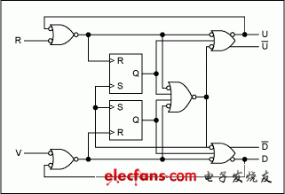
Figure 1. The MAX9382 frequency/phase detector.
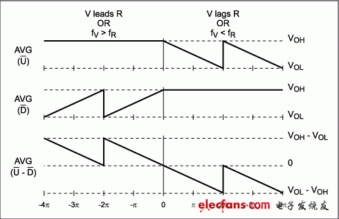
Figure 2. Ideal response of the MAX9382 frequency/phase detector.
Charge pump based loop filtering
Figure 3 shows a typical charge pump and passive loop filter architecture. This architecture uses switches to select matched current sources and current sinks to control the current flowing into or out of the loop filter. Pulses of different pulse widths are generated at the "upper" and "lower" outputs according to the phase difference of the phase detector input, causing the loop filter voltage to rise or fall. Under locked conditions, the phase detector generates a series of pulse signals with the same pulse width (minimum pulse width) at the two inputs of the charge pump. Equations 4 and 5 show the transfer function of the charge pump filter and the impedance of the loop filter network.
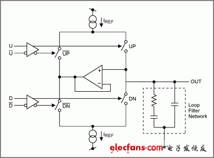
Figure 3. Charge pump and loop filter schematic.
Complete Phase-Locked Loop (PLL)
Figure 4 shows a complete phase-locked loop block diagram, which consists of a phase detector, charge pump, loop filter, VCO, and feedback divider (when required). Equation 6 shows the basic loop transfer function, and Equation 7 shows the complete loop transfer function under locked conditions. Equations 1 to 7 are derived from linear responses under different loop components, without considering the sampling characteristics of the phase detector and charge pump.
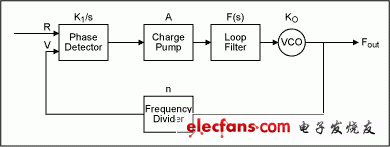
Figure 4. Basic unit of a phase-locked loop.
PLL Jitter and Frequency Response
Eliminate dead zone effect
A potential drawback of charge-pump-based phase-locked loops is that the minimum pulse width that the filter input can respond to is limited. Under phase-lock conditions, the typical phase detector output is a series of very short "up" and "down" output pulses. If these pulses are too narrow for the loop filter, a dead-zone effect will be generated around zero phase. This dead-zone effect will cause phase shift and increase jitter in the phase-locked output clock. Some systems will deliberately introduce a certain amount of phase shift to keep the phase detector output away from the deadlock region. The MAX9382 avoids the dead-zone effect by defining appropriate minimum "up" and "down" output pulses. Figure 5 shows the input and output timing of the MAX9382 when the VCO signal (V) leads the reference input signal (R). In this case, the phase detector outputs a series of narrow pulses at its "up" terminal (U) and a series of wide pulses at its "down" terminal (D). The difference between the "up" and "down" output pulse widths is the required V and R input transition time difference.
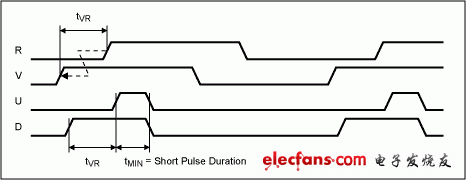
Figure 5. MAX9382 input and output timing when V leads R.
The minimum pulse width to avoid the dead-zone effect is mainly determined by the minimum input pulse width of the charge pump and the rise and fall characteristics of the phase detector output pulse. Equation 8 is used to calculate the approximate value of the minimum pulse width. The MAX9382 specification guarantees a minimum output pulse width of 370ps and a maximum output rise/fall time of 190ps. The minimum input pulse width for a specific loop filter is calculated using Equation 8, and the result is 360ps. Any loop filter with a minimum input pulse width below this value can be used with the MAX9382 to form a loop without the dead-zone effect.
Figure 6 illustrates the effect of a loop phase response of approximately zero and a very small minimum pulse width. Two responses are shown, both with the loop filter operating at 100MHz, requiring a 200ps input pulse width, and the phase detector output having a rise and fall time of 190ps. The first response is for a phase detector with a minimum output pulse width of approximately 0ps, and the second response is for a phase detector with a minimum output pulse width (in this case, the MAX9382 has a minimum pulse width of 370ps).
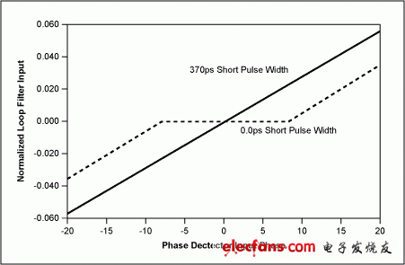
Figure 6. Comparison of loop dead-zone effects when the phase detector output pulse width is 370ps and 0.0ps
Maximum operating frequency
The MAX9382 data sheet gives a typical maximum operating frequency of 450MHz for an available input phase range of ±π. In a specific application, the maximum operating frequency is determined by the device's internal propagation delays and the available input phase range. An internal reset pulse is used to control the minimum output pulse width. If the reset pulse is valid when the next valid input edge is received, the phase detector will miss this input edge. The duration of this reset pulse is not specified in the MAX9382 data sheet, but its effective value can be calculated based on the input and output delays. For example, when the "V" input leads the "R" input, the limit of the input phase range is reached when the falling edge of the "D" output is aligned with the rising edge of the "V" input; for the case where the "R" input leads the "V" input, a similar situation occurs between the "R" input and the "U" output. Equation 9 gives an approximate expression for the maximum input phase when "V" leads "R". Figure 7 shows the corresponding timing diagram. The same expression and waveform can be given for the case where "R" leads "V".
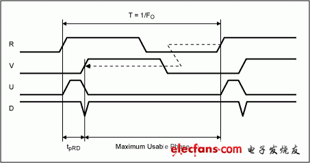
Figure 7. Device timing characteristics give maximum usable phase limits.
The timing diagram in Figure 7 depicts the input and output waveforms for the maximum phase condition. Further increasing the leading input phase will cause the subsequent rising edge of the “V” input to be ignored and the outputs to reset to a differential low state. The phase detector will respond to the next rising edge of the input as the leading waveform. In the example in Figure 7, the subsequent edge will appear at the “R” input and the phase detector response is for the condition where “R” leads “V”.
Formula List
Equations 1, 2, and 3 give the transfer functions of the phase/frequency detector under the same input frequency conditions (locked condition) and different input frequency conditions (corresponding to fV > fR, fV < fR).
in:
Output = Phase detection output
KP = Phase-detection gain
ΘR = reference signal phase
ΘV = feedback signal phase
in:
KF = Frequency Discriminator Gain
fR = reference signal frequency
fV = feedback signal frequency
Equations 4 and 5 give the transfer functions of the charge pump and loop filter.
in:
OUT = filter output
A = Gain (transconductance)
ZFILTER = filter network impedance
ΔT/T = “Up” and “Down” input duty cycle
in:
T1, T2, T3 = time constants associated with loop filter components
Equation 6 is the basic loop transfer function.
in:
FOUT = Loop output
R = Loop Input
n = feedback loop division ratio
K1 = Phase-locked transmission gain
K0 = VCO transfer gain
A = Charge Pump Gain
F(s) = loop filter transfer function
s = jω
Equation 7 is the complete loop transfer function under loop locked conditions.

Equation 8 is an approximation of the minimum pulse width to avoid the dead-time effect.

in:
PulseMIN = Minimum pulse width required at the phase detector output
tF = Phase detector output fall time (20% to 80%)
tR = Phase detector output rise time (20% to 80%)
tL = minimum input pulse width of loop filter
Equation 9 gives the maximum input phase range as a function of the operating frequency and the phase detector delay.
in:
ΘMAX = Maximum input phase
tpRD = propagation delay from R input to D output
F0 = Operating frequency
Previous article:Frequency Selective Amplifier Design
Next article:Introduction to Hall Sensor Applications
- High signal-to-noise ratio MEMS microphone drives artificial intelligence interaction
- Advantages of using a differential-to-single-ended RF amplifier in a transmit signal chain design
- ON Semiconductor CEO Appears at Munich Electronica Show and Launches Treo Platform
- ON Semiconductor Launches Industry-Leading Analog and Mixed-Signal Platform
- Analog Devices ADAQ7767-1 μModule DAQ Solution for Rapid Development of Precision Data Acquisition Systems Now Available at Mouser
- Domestic high-precision, high-speed ADC chips are on the rise
- Microcontrollers that combine Hi-Fi, intelligence and USB multi-channel features – ushering in a new era of digital audio
- Using capacitive PGA, Naxin Micro launches high-precision multi-channel 24/16-bit Δ-Σ ADC
- Fully Differential Amplifier Provides High Voltage, Low Noise Signals for Precision Data Acquisition Signal Chain
- Innolux's intelligent steer-by-wire solution makes cars smarter and safer
- 8051 MCU - Parity Check
- How to efficiently balance the sensitivity of tactile sensing interfaces
- What should I do if the servo motor shakes? What causes the servo motor to shake quickly?
- 【Brushless Motor】Analysis of three-phase BLDC motor and sharing of two popular development boards
- Midea Industrial Technology's subsidiaries Clou Electronics and Hekang New Energy jointly appeared at the Munich Battery Energy Storage Exhibition and Solar Energy Exhibition
- Guoxin Sichen | Application of ferroelectric memory PB85RS2MC in power battery management, with a capacity of 2M
- Analysis of common faults of frequency converter
- In a head-on competition with Qualcomm, what kind of cockpit products has Intel come up with?
- Dalian Rongke's all-vanadium liquid flow battery energy storage equipment industrialization project has entered the sprint stage before production
- Allegro MicroSystems Introduces Advanced Magnetic and Inductive Position Sensing Solutions at Electronica 2024
- Car key in the left hand, liveness detection radar in the right hand, UWB is imperative for cars!
- After a decade of rapid development, domestic CIS has entered the market
- Aegis Dagger Battery + Thor EM-i Super Hybrid, Geely New Energy has thrown out two "king bombs"
- A brief discussion on functional safety - fault, error, and failure
- In the smart car 2.0 cycle, these core industry chains are facing major opportunities!
- The United States and Japan are developing new batteries. CATL faces challenges? How should China's new energy battery industry respond?
- Murata launches high-precision 6-axis inertial sensor for automobiles
- Ford patents pre-charge alarm to help save costs and respond to emergencies
- New real-time microcontroller system from Texas Instruments enables smarter processing in automotive and industrial applications
- Building ESP32-C3 development environment based on window Visual Studio Code: ESP-IDF
- [AT-START-F403A Review] + Unsuccessful W25Q128 Read and Write
- Cadence Allegro beginners must read
- EEWORLD University ---- Introduction to CC2650MODAPluetooth? Low-energy RF module
- After the microcontroller is powered on, it runs a display program and encounters a very strange problem.
- A brief discussion on LTE technology and practical application solutions
- What is the drilling process in the Siliton ceramic substrate PCB?
- SD/TF card usage issues
- Download address of Arteli technical resources
- MSP430F249 external interrupt P1.3 port

 Introduction to the classification, application, composition and model of phase-locked loop


 京公网安备 11010802033920号