Here we are going to talk about the configuration circuit of Xilinx's spartan-3 series FPGA. Of course, the configuration circuits of other series of FPGAs are similar, and readers can make inferences and focus on the official datasheet, which is the most authoritative information after all.
As for typical, here is a list of the most common spartan-3 xc3s400 configuration circuits on the market. The connection method of all spartan-3 FPGA configuration circuits is the same. Xc3s400 is a 400,000-gate FPGA. Although its Configuration Bitstream is only 1.699136Mbit, it still needs a 2Mbit configuration chip XCF02S. You can't take it for granted that my design is simple and only uses 1Mbit at most, so I can choose XCF01S (1Mbit). This is not the case. Even if you only use xc3s400 to design a running light, the data you download to the ROM (XCF02S) is also 1.699136Mbit, so it is better to choose a larger configuration ROM for the FPGA rather than a smaller one.
There are five types of configuration circuits: master serial, slave serial, master parallel, slave parallel, and JTAG. The first four are relative to downloading to PROM (serial and parallel are relative to the serial and parallel protocols and FPGA communication of different configuration chips), and only JTAG is relative to debugging, which is to download the configuration to the RAM of FPGA (lost after power failure). Compared with FPGA and CPLD, CPLD is based on ROM, that is, after the data is downloaded to CPLD, it will not be lost after power failure. FPGA is based on RAM. If there is no external ROM to store configuration data, the data will be lost after power failure. Therefore, FPGAs need to have external configuration chips (of course, there are also FLASH-based FPGAs now). Then let's take a look at the connection of the configuration circuit of FPGA in master serial mode.
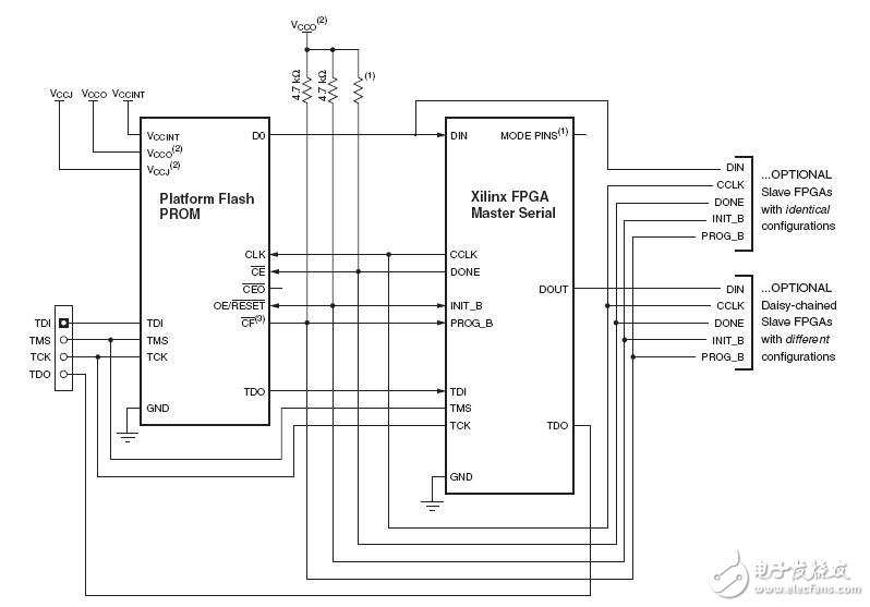
The official hardware connections are as follows :

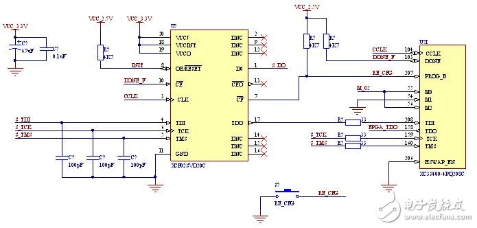
In order to increase the reliability of the configuration circuit, we usually add some anti-interference designs (such as adding filter capacitors and matching resistors):

Let's look at the various pins of the PROM chip first. I won't talk about pins 18, 19, and 20. The corresponding voltage levels are given according to the datasheet. Pin 3 CLK is connected to the CCLK of the FPGA, and the synchronization of data communication is carried out through the clock generated by the CCLK of the FPGA. Because the chip used is a serial configuration chip, there is only one data signal port DO, which is connected to the DIN port of the FPGA (not shown in the above figure), and works with the clock signal above to complete serial data transmission. Every time the rising edge of CLK latches data, the address counter inside the PROM automatically increases. There are also two control signal lines, INIT (connected to the OE/RESET of the PROM) and DONE (connected to the CE of the PROM). OE/RESET is to ensure that the address counter of the PROM is reset before each reconfiguration. Regarding the CE pin, the official information is not very detailed. In my personal understanding, CE should be chip The abbreviation of enable. From its connection with the DONE pin of FPGA, we can easily infer that when FPGA is not configured, DONE=0, then the configuration chip PROM is in the chip select state, and once the configuration is completed, DONE=1, then the PROM is no longer selected. At the same time, the datasheet also says that this pin can be directly grounded, that is, it is always chip selected, but this will cause the DATA port to have continuous data signal output and cause unnecessary current consumption; the CEO pin is not connected here, because it is used as the OE terminal signal connection of the next PROM in the configuration circuit of multiple PROMs; the CF signal is connected to the PROG_B interface of FPAG, and its function is to generate a start configuration signal. It is connected to a pull-up resistor. If PROG_B generates a low-level pulse, the PROM will restart the configuration, so we will connect a button to the ground on this line. If the button is pressed, the PROM will be enabled to reconfigure the FPGA; there are also several signal interfaces TDI, TCK, TMS, TDO, which are signals connecting PROM and PC. PC downloads data to PROM through these circuits (usually connected to a driver isolation chip and communicated through the parallel port, which is not emphasized here).
When we talked about the signal interface of PROM above, we also talked about the configuration pins of FPGA. Here are some summary explanations. FPGA has 7 dedicated configuration pins (CCLK, DIN, PROG_B, DONE, HSWAP_EN, M0, M1, M2), 4 dedicated JTAG pins (TDI, TCK, TMS, TDO), these pins are powered by VCCAUX (this series of FPGA is usually connected to VCCAUX = 2.5V). The M0, M1, and M2 pins of FPGA are used for configuration mode selection. In the main serial mode of this circuit, {M0, M1, M2} = 000, if it is JTAG download mode {M0, M1, M2} = 101. The HSWAP_EN pin not mentioned above is grounded, which is used to set other idle pins to pull-up state when FPAG is in the configuration state. If this pin is connected to a high level, other idle pins will float when FPAG is in the configuration state. Therefore, in order to reduce interference in the FPGA configuration process, this pin is generally grounded.
Previous article:Cypress PSoC4 chip secrets: Play with SAR ADC module
Next article:Mobile High-Definition Link (MHL) technology adopted by 200 equipment manufacturers worldwide
Recommended ReadingLatest update time:2024-11-16 14:36


- Popular Resources
- Popular amplifiers
-
 Analysis and Implementation of MAC Protocol for Wireless Sensor Networks (by Yang Zhijun, Xie Xianjie, and Ding Hongwei)
 -
 MATLAB and FPGA implementation of wireless communication
 -
 Intelligent computing systems (Chen Yunji, Li Ling, Li Wei, Guo Qi, Du Zidong)
 -
 Summary of non-synthesizable statements in FPGA
- High signal-to-noise ratio MEMS microphone drives artificial intelligence interaction
- Advantages of using a differential-to-single-ended RF amplifier in a transmit signal chain design
- ON Semiconductor CEO Appears at Munich Electronica Show and Launches Treo Platform
- ON Semiconductor Launches Industry-Leading Analog and Mixed-Signal Platform
- Analog Devices ADAQ7767-1 μModule DAQ Solution for Rapid Development of Precision Data Acquisition Systems Now Available at Mouser
- Domestic high-precision, high-speed ADC chips are on the rise
- Microcontrollers that combine Hi-Fi, intelligence and USB multi-channel features – ushering in a new era of digital audio
- Using capacitive PGA, Naxin Micro launches high-precision multi-channel 24/16-bit Δ-Σ ADC
- Fully Differential Amplifier Provides High Voltage, Low Noise Signals for Precision Data Acquisition Signal Chain
- Innolux's intelligent steer-by-wire solution makes cars smarter and safer
- 8051 MCU - Parity Check
- How to efficiently balance the sensitivity of tactile sensing interfaces
- What should I do if the servo motor shakes? What causes the servo motor to shake quickly?
- 【Brushless Motor】Analysis of three-phase BLDC motor and sharing of two popular development boards
- Midea Industrial Technology's subsidiaries Clou Electronics and Hekang New Energy jointly appeared at the Munich Battery Energy Storage Exhibition and Solar Energy Exhibition
- Guoxin Sichen | Application of ferroelectric memory PB85RS2MC in power battery management, with a capacity of 2M
- Analysis of common faults of frequency converter
- In a head-on competition with Qualcomm, what kind of cockpit products has Intel come up with?
- Dalian Rongke's all-vanadium liquid flow battery energy storage equipment industrialization project has entered the sprint stage before production
- Allegro MicroSystems Introduces Advanced Magnetic and Inductive Position Sensing Solutions at Electronica 2024
- Car key in the left hand, liveness detection radar in the right hand, UWB is imperative for cars!
- After a decade of rapid development, domestic CIS has entered the market
- Aegis Dagger Battery + Thor EM-i Super Hybrid, Geely New Energy has thrown out two "king bombs"
- A brief discussion on functional safety - fault, error, and failure
- In the smart car 2.0 cycle, these core industry chains are facing major opportunities!
- The United States and Japan are developing new batteries. CATL faces challenges? How should China's new energy battery industry respond?
- Murata launches high-precision 6-axis inertial sensor for automobiles
- Ford patents pre-charge alarm to help save costs and respond to emergencies
- New real-time microcontroller system from Texas Instruments enables smarter processing in automotive and industrial applications
- Questions about vhdl testbench
- Can the AGND and DGND pins of VS1053 be connected directly?
- [NXP Rapid IoT Review] Online IDE Development Experience
- FAQ_How to solve the ADC sampling accuracy problem in BlueNRG-12
- Ultrasonic standing wave axial suspension moving device
- 8. Contents that students need to master
- EEWORLD University ---- TI Precision Labs - ADC: 9.7 High-Speed Data Converter Signal Processing: Real and Complex Modulation
- EEWORLD University Hall----Live Replay: Renesas Electronics Secure IoT Suite provides you with secure cloud connection solutions
- SD NAN storage solution for single chip hunting camera products
- MSP430 program upgrade method

 Analysis and Implementation of MAC Protocol for Wireless Sensor Networks (by Yang Zhijun, Xie Xianjie, and Ding Hongwei)


 京公网安备 11010802033920号