Video surveillance is widely used in many occasions because of its intuitiveness, convenience and rich information content. Video surveillance has become an indispensable technology in people's lives. In some dangerous places, video surveillance can replace manual surveillance to ensure people's life safety. Given that the field of view of one video is limited, in order to fully collect information about the target, it is necessary to have multiple videos to monitor the same object in different directions. Therefore, a good control method is needed to ensure that the multi-channel video control is stable and reliable. In response to the needs of the loom alarm system, a multi-channel video channel control system based on FPGA is proposed. This system design uses FPGA to indirectly control the required video channels of two MAX4312s to switch between each video channel. According to the design idea of the switch control signal, the input signal of the toggle switch is jittered in the FPGA, and then different switch operations are encoded, and finally the signal is sent to the DSP for processing.
l Overall system structure
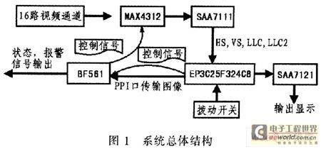
The overall structure of the system is shown in Figure 1. 16 CCD image sensors are installed on an industrial loom to monitor the cloth. One of the 16 image video signals is selected through two MAX4312s. After being processed by the programmable video input device SAA7111, the digital image signal is output from VP0. At the same time, SAA7111 outputs the corresponding line and field synchronization signals HS, VS and the clock signals LLC and LLC2 locked with HS. These signals are used to pre-process the image in EP3C25F324C8. Then the processed image is sent to BF561 through the PPI port for algorithm processing, and finally the processing result is sent to the alarm and status indication device to realize the alarm function of the loom. In order to make image monitoring more convenient, the system design adds a level toggle switch and a pulse toggle switch. The level switch stops the input image from switching and is fixed to one of the video input images. The pulse switch can be toggled left or right. Each time it is toggled left or right, a very short rising edge pulse will be generated, and the image will switch forward or backward at the same time, realizing the function of manually selecting the video input channel.
2 Software Module Design
2.1 Switch control signal
In actual projects, BF561 has relatively few PF pins connected to FPGA. In order to save resources, only BF9 in BF561 is used to identify the actions of the two slide switches. Therefore, the input signals of the two slide switches need to be processed and integrated in FPGA to obtain appropriate signals.
The design idea of the switch control signal of this system: Since the purpose of designing this signal is to identify the switch control action. Therefore, a pulse needs to be generated as long as any switch is activated. If there is only a pulse signal, we can only know that the switch has been activated, but we don’t know which switch has been activated. Therefore, to identify which specific switch has been activated, it is necessary to decode it with the data in the dual-port RAM. The pulse duration designed by this system is not important for BF561, as long as BF561 can recognize this pulse. Since there are two toggle switches in the system, one is a level toggle switch and the other is a pulse toggle switch, therefore, as long as the corresponding pulse signal is made according to the action of the level toggle switch, and then this signal is logically ANDed with the original signal generated by the pulse toggle switch, the desired target signal can be obtained.
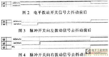
Since the toggle switch is a mechanical contact, there will be corresponding leading and trailing edge jitter when it is opened and closed. In order to make each action respond only once, the original switch signal must be jittered. Jitter signals can be divided into two types: one is a very short interference signal, such as high-frequency burrs; the other is a longer interference signal, such as switch jitter. The toggle switches here are all manually operated, so the time of each trigger will not be very short, generally less than 10 Hz. According to the above analysis, the switch jitter signal belongs to the latter. Therefore, after each switch operation, the signal generated is continuously sampled. If each sampling is low level or high level, it is considered that the signal is not jitter, and the switch state has indeed changed. The entire design process is written in Verilog hardware description language, then compiled on the QuartusⅡ platform, and SignalTapⅡLogic Arlalvzer is used to sample and analyze the signal. After debugging, it is burned into the FPGA configuration device EPCSl6 together with other programs. Figures 2 to 4 are real-time signal sampling diagrams before and after the jitter of each switch action. Some of the codes in the jitter module are as follows:
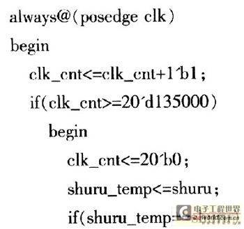
Where clk is a 13.5 MHz clock signal, clk_cnt is a sampling time interval counter, and sampling is performed once when clk_cnt is 135 000, i.e., once every 10 ms. The register shuru_temp stores the previous switch signal state, and shum stores the current switch signal state. If the value of shuru_temp is the same as the value of shtlm, the counter test_cnt automatically increases by 1. If the sampling values are equal for four consecutive times, i.e., when test_cnt=4, the jitter output will change with the input.
Using the level toggle switch signal as input, a pulse signal is produced to identify the switch action. The code is as follows:
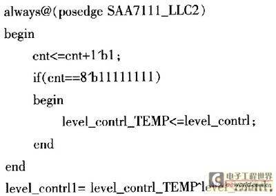
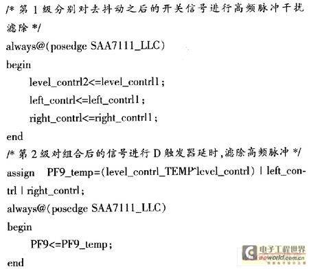
In the code, the register level_contrl_TEMP stores the signal of level_contrl after delaying 256 clock cycles, and then uses the signal stored in level_eontrl_TEMP to differ from the value of level_co-ntrl or generate the required pulse signal.
During debugging, it was found that the jittered signal was often mixed with high-frequency pulse interference signals of very short duration. Therefore, a two-stage D flip-flop delay was used in the design to completely eliminate the high-frequency pulse interference. The program code is as follows:
2.2 Dual-port RAM and switch signal encoding design
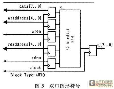
Dual-port RAM is divided into two types: true and false. The two ports of a true dual-port can be read and written without interfering with each other. In this design, according to actual needs, one end of the added RAM module is read-only and the other end is write-only, and the reading and writing do not interfere with each other. According to the above analysis, the switch control signal can only know that a switch control action has occurred, but cannot identify which specific switch has been acted. Therefore, in the design, the macro function block RAM: 2_PORT in MegaWizardPlug_In Manager is first used to generate a dual-port RAM storage block, and then the parameters of this macro function module are appropriately adjusted to generate a module that meets one's specific requirements, as shown in Figure 5.
During the design process, the switch action is first encoded. The encoded data is then stored in a dual-port RAM with a space size of 8. When BF561 detects the pulse on PF9, it reads the data at the specified address in the RAM in the PF interrupt, then decodes the switch state based on this data and manipulates the two MAX4312 devices according to the decoded control information to control the video channel. The encoding program code for the switch action is as follows:
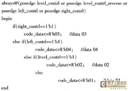
The whole design has 4 switch actions, which are encoded into data 01, 02, 03, and 04 in the program, and then stored in the dual-port module, waiting for BF561 to read and decode. Figure 6 is the sampling of the data stored in RAM after the pulse switch is toggled to the right in SignalTapⅡLogic Analyzer.

In the program, the RAM read signal rden_signal is controlled by the address signal DSP_A, the BANK selection signal DSP_AMS1 and the DSP read signal DSP_ARE sent by the DSP. When the DSP does not read data from the dual port, the DSP data line must be assigned a high impedance to avoid affecting the SDRAM's manipulation of the DSP data line. The assignment instruction is as follows: assignDSP_D=(rden_signal=l'b1)? DSP_D_TEMP; 8 'hzz; where DSP_D_TEMP is the data read from the dual port.
3 Conclusion
First, the industrial background and hardware architecture of the whole system are introduced, and then the focus is on how to process the switch control signal in FPGA to achieve the purpose of reliable response to each switch action. The whole design program is written in Verilog hardware description language on QuartusⅡ platform, and the download tool and SignalTapⅡLogic Analyzer tool in QuartusⅡ are used for downloading, real-time sampling, and multiple debugging and verification. This design has been successfully applied to the machine alarm system, and each time the switch is turned on, the video channel can be switched correctly and reliably. Although there are only two types of switches in this system, the design concept of the whole program is also universal for multiple switch controls, and multiple switch actions can be recognized by only slight changes in the details.
Previous article:Multi-DSP Infrared Real-time Image Processing System Based on FPGA
Next article:FPGA Design of Digital Signal Processor Based on DSP Builder
- Popular Resources
- Popular amplifiers
- Huawei's Strategic Department Director Gai Gang: The cumulative installed base of open source Euler operating system exceeds 10 million sets
- Analysis of the application of several common contact parts in high-voltage connectors of new energy vehicles
- Wiring harness durability test and contact voltage drop test method
- Sn-doped CuO nanostructure-based ethanol gas sensor for real-time drunk driving detection in vehicles
- Design considerations for automotive battery wiring harness
- Do you know all the various motors commonly used in automotive electronics?
- What are the functions of the Internet of Vehicles? What are the uses and benefits of the Internet of Vehicles?
- Power Inverter - A critical safety system for electric vehicles
- Analysis of the information security mechanism of AUTOSAR, the automotive embedded software framework
 Professor at Beihang University, dedicated to promoting microcontrollers and embedded systems for over 20 years.
- LED chemical incompatibility test to see which chemicals LEDs can be used with
- Application of ARM9 hardware coprocessor on WinCE embedded motherboard
- What are the key points for selecting rotor flowmeter?
- LM317 high power charger circuit
- A brief analysis of Embest's application and development of embedded medical devices
- Single-phase RC protection circuit
- stm32 PVD programmable voltage monitor
- Introduction and measurement of edge trigger and level trigger of 51 single chip microcomputer
- Improved design of Linux system software shell protection technology
- What to do if the ABB robot protection device stops
- Allegro MicroSystems Introduces Advanced Magnetic and Inductive Position Sensing Solutions at Electronica 2024
- Car key in the left hand, liveness detection radar in the right hand, UWB is imperative for cars!
- After a decade of rapid development, domestic CIS has entered the market
- Aegis Dagger Battery + Thor EM-i Super Hybrid, Geely New Energy has thrown out two "king bombs"
- A brief discussion on functional safety - fault, error, and failure
- In the smart car 2.0 cycle, these core industry chains are facing major opportunities!
- The United States and Japan are developing new batteries. CATL faces challenges? How should China's new energy battery industry respond?
- Murata launches high-precision 6-axis inertial sensor for automobiles
- Ford patents pre-charge alarm to help save costs and respond to emergencies
- New real-time microcontroller system from Texas Instruments enables smarter processing in automotive and industrial applications
- Understanding the past, present and future of the Matter Protocol in one article
- Schematic diagram of various application circuits of LM324
- [Voice and vision module based on ESP32S3]-The materials have not arrived yet, so use ESPcam to test QR code recognition first
- Circuit Schematic Analysis Method
- Hongmeng Development Board Neptune (Part 3) - Problems encountered in the development environment
- Live broadcast at 10:00 am today [Unlocking new possibilities of TI Sitara AM2x MCU in motor drive]
- 3.5mm audio interface type description
- Is wireless charging technology for new energy vehicles really not working?
- Introduction to flow principle in automatic monitoring system of oil and gas recovery in oil stations
- Op amp

 MAX44284WAWT+


 京公网安备 11010802033920号