In the field of software radio and communications, orthogonal digital signals are often used. For such applications, this paper presents an FPGA-based orthogonal NCO design method that can realize an orthogonal, continuous phase, high-performance, high-precision, reusable numerically controlled oscillator, which is suitable for the design of on-chip systems in a variety of application scenarios.
1 NCO Implementation Principle
Direct digital frequency synthesis (DDS) technology is a fully digital technology. Compared with traditional frequency synthesis technology, DDS technology has many advantages: short frequency switching time, high frequency resolution, continuous phase change, and easy implementation of various modulations of the output signal.
The principle block diagram of DDS is shown in Figure 1. Its essence is to sample the phase at equal intervals with the reference frequency source (system clock). As can be seen from Figure 1, DDS consists of three parts: a numerically controlled oscillator (NCO) composed of a phase accumulator and a waveform memory (ROM lookup table), a digital-to-analog converter (DAC), and a low-pass filter (LPF). The core of DDS is the design and implementation of NCO. NCO is generally composed of two parts: a phase accumulator and a sine-cosine lookup table. The design of the phase accumulator is relatively simple, so the key to designing NCO is to design the sine and cosine function generators.
The method to implement the function generator is the lookup table method (LUT). For an NCO with L phase bits and M output signal amplitude bits, the required lookup table size is M×2L.
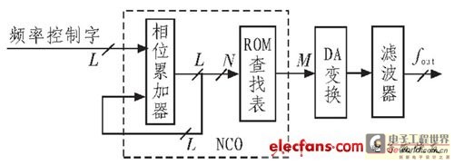
Figure 1 DDS basic principle block diagram
In each clock cycle, the L-bit phase accumulator and its feedback value are accumulated, and the high N bits of the result are used as the address of the ROM lookup table, and then the corresponding amplitude value is read out from the ROM and sent to the DAC. The low-pass filter LPF is used to filter out the high-order harmonics in the DAC output. Therefore, the output frequency fout can be changed by changing the frequency control word K. It is easy to get the relationship between the output frequency fout and the frequency control word K: fout=Kfc/2L, where fc is the clock frequency of the phase accumulator and L is the number of bits of the phase accumulator. Define when K=1 as the system frequency resolution, that is, f=fc/2L.
2. Several common NCO design methods
Common NCO implementation methods currently include calculation method, CORDIC (Coordinated Rotation Digital Computer) algorithm and table lookup method.
The calculation method is a software programming method that generates sine wave samples through real-time calculation. This method is time-consuming and can only generate sine waves with relatively low frequencies. When high-speed orthogonal signals need to be generated, this method cannot meet the requirements well.
The CORDIC algorithm is a digital calculation method for coordinate rotation. Its basic idea is to use a series of fixed-angle continuous deflections to approximate the required rotation angle, and to achieve multiplication, division, square roots, trigonometric functions, vector rotation (complex multiplication) and exponential operations. This algorithm often requires multipliers and lookup tables to calculate a variety of transcendental functions, which will lead to complex hardware circuit implementation and reduced computing speed. In addition, the angle range it can calculate is also limited, so the CORDIC algorithm has greater restrictions in actual use.
In practical applications, the most effective and simple table lookup method is generally used, that is, the sine value of the phase is calculated in advance according to the phase of each NCO sine wave, and the sine value data of the phase is stored in the table with the phase angle as the address, and then the address information is generated by phase accumulation to read the sine value corresponding to the current phase value in the table, thereby generating a sine wave of the required frequency; at the same time, due to the symmetry of the sine and cosine waveforms, only part of the data needs to be stored to complete the numerical output of the full phase. This implementation method is simple in design and has a high operating speed, and can well meet the requirements of various occasions such as digital frequency conversion, spread spectrum, modulation and demodulation.
3. Orthogonal NCO Lookup Table Implementation Method
The principle block diagram of the FPGA-based orthogonal NCO design is shown in Figure 2. It mainly consists of three parts: a variable modulus counter, a sine-cosine lookup table, and an output unit.

Figure 2 NCO design principle block diagram
The following design is based on the example of input frequency control word 1200 Hz.
Fre_sample indicates that the system uses a clock; Fre_cnt_word indicates the frequency control word.
1) Design of variable modulus counter
The variable modulus counter calculates the address required for the sine and cosine table lookup based on the frequency control word; at the same time, it is necessary to ensure that the phase of the generated sine and cosine waves remains continuous (some applications often require the output phase to be continuous), that is, to set the corresponding remainder value. The frequency control word is read in the first working clock cycle, mod (Fre_sample, Fre_cnt_word) is calculated as the phase control word in the second working clock cycle, the internal counter is reset and the phase control word is entered in the third working clock cycle, and the counting output starts from the fourth clock cycle with the frequency control word as the step length and the phase control word as the initial value.
2) Design of sine and cosine lookup table
The sine-cosine lookup table obtains the output of the corresponding carrier frequency waveform by looking up the output of the variable modulus counter.
A key to the design of NCO based on FPGA is that the output address of the waveform memory ROM phase accumulator is used as the address input of the ROM. After table lookup and calculation, the ROM outputs the quantized data of the sine and cosine waveforms. The design mainly aims to save the memory resource overhead, that is, to reduce the space of the ROM storage table. Since the size of the storage table increases exponentially with the increase of the number of address bits or data bits, the overhead of the smaller ROM storage table is mainly considered under the premise of meeting the frequency resolution and signal performance. In practical applications, the symmetry of the sine and cosine signals within a cycle can be fully utilized to reduce the overhead of the ROM storage table. For example, the sine signal is symmetrical about the X-axis within a cycle. Based on this, the ROM storage table can be reduced to 1/2 of the original size. Then, the left-right symmetry within a half cycle can be used to reduce the ROM storage table to 1/2 of the original size. Therefore, the first 1/4 cycle of a sine lookup table can be transformed to obtain the entire sine wave cycle lookup table, thus saving 3/4 of the memory resources.
The specific design idea of the sine and cosine table is as follows: take the frequency resolution as df=1 Hz; assume that the frequency control word is around 1200 Hz, and now consider taking 8 samples for each cycle of the 1200 Hz sine and cosine waveform, then the sampling rate is fs=1200×8=9600 Hz. Assume that 8 bits are used for quantization of each sample value, then each table needs to store a total of 9.6 kB; (if the symmetry of the sine and cosine signals is taken into account, the design can be optimized to store 1/4 of the waveform in each table, that is, each table only needs to store 2.4 kB;) When in use, the step size STep is used to adjust the output frequency, while ensuring the phase continuity of the output sine and cosine waves. If every 0 sample point is taken as 1, that is, step=1, the output frequency is 1 Hz; every 1 point is taken as 1, that is, step=2, the output frequency is 2 Hz; ...; every 1199 points is taken as 1, step=1200, the output frequency is 1200 Hz.[page]
3) Loading the sine and cosine table
The mif file format in Quartus software can be used to conveniently load the storage table; at the same time, MATLAB output can be used to generate the loading file. The mif file format is very convenient to generate; as shown below, a mif file with a bit width of 8 bits, a depth of 9,600, an unsigned address, and decimal data of 9,600 units is given. When initializing RAM, just follow the guidance of Quartus software to directly configure it.
WIDTH=8;
DEPTH=9600;
ADDRESS_RADIX=UNS;
DATA_RADIX=DEC;
CONTENT BEGIN
0 : 0;
1 : 2;
2 : 10;
3 : 30;
4 : 50;
5 : 50;
6 : 10;
7 : 100;
……
9598 : 0;
9599 : 0;
END
4 Design implementation and simulation waveform
This design uses the cost-effective STRATIX chip of ALTERA for design simulation. This series of chips is an FPGA chip based on 1.5 V working voltage and 0.13 μm full copper wiring SRAM process. This series of chips has up to 114 140 logic units (LEs) and up to 10 Mbits of internal RAM. This series of chips supports multiple I/O standards and provides up to 12 phase-locked loops (PLLs) for processing complex clock signals. At the same time, the STRATIX series of chips provides up to 28 digital signal processing units (DSPs), which are composed of a total of 224 built-in hardware multipliers (9 bits by 9 bits). They can be used to effectively implement high-performance digital signal processing units or multipliers such as fast Fourier transform (FFT), finite impulse response (FIR) filter, infinite impulse response (IIR) filter, etc.
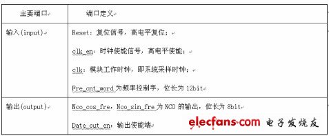
Figure 3 Main port definitions of the NCO module
2) Quartus simulation output waveform, as shown in Figure 4.

Figure 4 NCO simulation output waveform
This simulation waveform is the NCO output waveform of three frequency points. The waveform of the output carrier drawn by matlab is shown in Figure 5.
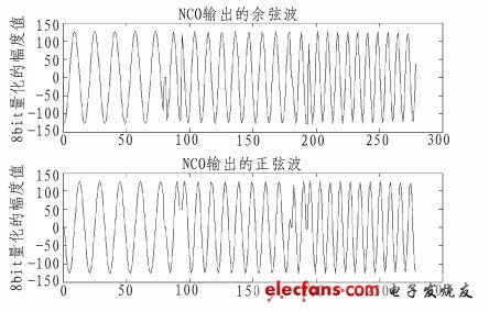
Figure 5 Output carrier waveform
From the above simulation results, we can see that the NCO correctly outputs the simulation waveforms of the three frequency points; at the same time, through actual FPGA hardware testing and verification, the design has achieved the required performance indicators. [page]
5 Resource usage
Altera's STRATIX chip is used for compilation and synthesis, and the resource usage results are shown in Figure 6.
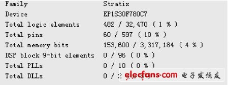
Figure 6 NCO resource usage
6 Conclusion
This article presents a design method for an orthogonal NCO based on FPGA. In actual application, you can refer to the given design example. By changing the frequency control word, system sampling frequency, the depth of the sine and cosine lookup table, and the bit width of the storage table, you can get NCOs with different input frequency ranges. At the same time, if the required accuracy and frequency are high, you can also use external memory, such as FLA5. Resource occupancy
Altera's STRATIX chip is used for compilation and synthesis, and the resource usage results are shown in Figure 6.

Figure 6 NCO resource usage
6 Conclusion
This paper presents a design method for an orthogonal NCO based on FPGA. In actual application, the design example given can be used as a reference. By changing the frequency control word, the system sampling frequency, the depth of the sine and cosine lookup table, and the bit width of the storage table, NCO with different input frequency ranges can be obtained. At the same time, if the required accuracy and frequency are high, external memory such as FLASH, SRAM, etc. can be used in conjunction with FPGA. The larger the depth and bit width of the extended storage table, the better the design requirements can be achieved.
SH, SRAM, etc. are used in conjunction with FPGA, and the larger depth and bit width of the extended storage table can ultimately meet the design requirements.
Previous article:How to choose a DSP chip?
Next article:Large-capacity data storage based on FPGA and external SRAM
Recommended ReadingLatest update time:2024-11-16 19:35


- Popular Resources
- Popular amplifiers
-
 Analysis and Implementation of MAC Protocol for Wireless Sensor Networks (by Yang Zhijun, Xie Xianjie, and Ding Hongwei)
 -
 MATLAB and FPGA implementation of wireless communication
 -
 Intelligent computing systems (Chen Yunji, Li Ling, Li Wei, Guo Qi, Du Zidong)
 -
 Summary of non-synthesizable statements in FPGA
- Huawei's Strategic Department Director Gai Gang: The cumulative installed base of open source Euler operating system exceeds 10 million sets
- Analysis of the application of several common contact parts in high-voltage connectors of new energy vehicles
- Wiring harness durability test and contact voltage drop test method
- Sn-doped CuO nanostructure-based ethanol gas sensor for real-time drunk driving detection in vehicles
- Design considerations for automotive battery wiring harness
- Do you know all the various motors commonly used in automotive electronics?
- What are the functions of the Internet of Vehicles? What are the uses and benefits of the Internet of Vehicles?
- Power Inverter - A critical safety system for electric vehicles
- Analysis of the information security mechanism of AUTOSAR, the automotive embedded software framework
 Professor at Beihang University, dedicated to promoting microcontrollers and embedded systems for over 20 years.
- Innolux's intelligent steer-by-wire solution makes cars smarter and safer
- 8051 MCU - Parity Check
- How to efficiently balance the sensitivity of tactile sensing interfaces
- What should I do if the servo motor shakes? What causes the servo motor to shake quickly?
- 【Brushless Motor】Analysis of three-phase BLDC motor and sharing of two popular development boards
- Midea Industrial Technology's subsidiaries Clou Electronics and Hekang New Energy jointly appeared at the Munich Battery Energy Storage Exhibition and Solar Energy Exhibition
- Guoxin Sichen | Application of ferroelectric memory PB85RS2MC in power battery management, with a capacity of 2M
- Analysis of common faults of frequency converter
- In a head-on competition with Qualcomm, what kind of cockpit products has Intel come up with?
- Dalian Rongke's all-vanadium liquid flow battery energy storage equipment industrialization project has entered the sprint stage before production
- Allegro MicroSystems Introduces Advanced Magnetic and Inductive Position Sensing Solutions at Electronica 2024
- Car key in the left hand, liveness detection radar in the right hand, UWB is imperative for cars!
- After a decade of rapid development, domestic CIS has entered the market
- Aegis Dagger Battery + Thor EM-i Super Hybrid, Geely New Energy has thrown out two "king bombs"
- A brief discussion on functional safety - fault, error, and failure
- In the smart car 2.0 cycle, these core industry chains are facing major opportunities!
- The United States and Japan are developing new batteries. CATL faces challenges? How should China's new energy battery industry respond?
- Murata launches high-precision 6-axis inertial sensor for automobiles
- Ford patents pre-charge alarm to help save costs and respond to emergencies
- New real-time microcontroller system from Texas Instruments enables smarter processing in automotive and industrial applications
- [Synopsys IP Resources] EDA on the cloud makes chip innovation "fast, accurate and stable"
- Internet of Vehicles testing and verification of automotive CAN bus network data
- Which manufacturers are there of domestic battery metering chips?
- Today at 10:00 am | TI Award Live Broadcast [DIY Home Monitoring Edge AI Box]
- [Raspberry Pi Pico Review] - Start compiling the program 2
- USB2.0 Transactions
- Characteristics of voltage-type electrostatic breakdown of MOS tubes
- EEWORLD University Hall----Live Replay: Protecting Clean Water Sources-ADI Water Quality Monitoring Solutions
- Share: How to convert C program from floating point to fixed point
- MicroPython major historical versions

 Analysis and Implementation of MAC Protocol for Wireless Sensor Networks (by Yang Zhijun, Xie Xianjie, and Ding Hongwei)


 京公网安备 11010802033920号