0 Introduction
The development of CMOS technology has made the integration of chips higher and higher, and the number of IOs on a single chip has also increased. When these chips are widely used in high-speed digital systems, synchronous switching noise becomes very prominent.
Synchronous switching noise (SSN) is generated by the simultaneous switching of IO output buffers, also known as synchronous switching output noise (SSO). One of the main reasons for SSO is the impedance of the power distribution system (PDS). Specifically, there is a distance from the output end of the power supply to the input end of the chip, and there is impedance on this path. From the perspective of the centralized model, it is equivalent to connecting concentrated distributed resistance and inductance elements in series. When a certain number of CMOS output drive circuits are turned on at the same time, a large current will instantly flow into these inductive elements. This instantaneous and rapid change of current will generate an induced electromotive force on the inductive element, causing the net supply voltage at the chip power input end to be insufficient or too high.
At present, the commonly used method is to add enough decoupling capacitors close to the power input end of the chip, which can play a role in voltage stabilization. However, since the power plane and the chip power plane are not effectively isolated, the noise interference on the power plane can easily enter the power plane of the chip, and finally conduct to the SSO, making the SSO worse. This paper proposes L-type and π-type LC filter circuit design schemes, which can effectively isolate the medium and high frequency noise interference between the two planes and improve the SSO problem. The following is a detailed introduction and analysis.
1 L-type LC power filter circuit
1.1 L-type LC power filter circuit model and working principle
The equivalent model of the L-type LC filter circuit is shown in Figure 1. The components of the entire equivalent model are inductor L and decoupling capacitor C1. The main function of inductor L is to suppress the jump of current and play a role in current stabilization. The main function of decoupling capacitor C1 is to suppress the jump of voltage caused by SSO and play a role in voltage stabilization. SSO can be equivalent to a current source of an instantaneous switch. In order to represent the worst case, that is, all IOs are turned on at the same moment, the current demand at this time is equal to the maximum operating current I of the chip at this voltage.
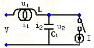
Figure 1 L-type LC power filter circuit
The working principle of this circuit is that when SSO is turned on at the same time, an instantaneous demand for current I is generated. First, C1 discharges to maintain a slow voltage change, and at the same time, the capacitor is charged through the inductor L. Through this repeated charging and discharging process, the voltage at the chip input is maintained within the error range of the chip's normal operating voltage. From the perspective of the spectrum, LC forms a low-pass filter, which effectively isolates the medium and high frequency noise between the two planes.
1.2 Algorithm analysis of L-type LC power supply filter circuit
According to the equivalent model of Figure 1, the equation group (I) can be obtained:
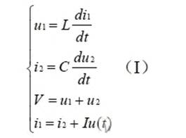
After simplifying the equation group (I), the second-order differential equation

(II) is obtained. Solving the differential equation (II) obtains a special solution:

If the voltage V is a constant, the special solution (III) is brought into the second-order differential equation (II) to obtain:

If the input voltage V contains ripple Vn sin(ωnt), then the solution is:

From (V), it can be seen that after passing through the LC filter circuit, the ripple is amplified, and the amplification factor is
![]() . Take
. Take
![]() the amplification factor as
the amplification factor as
![]()
When
![]() the LC circuit has a suppressive effect on the power supply ripple.
the LC circuit has a suppressive effect on the power supply ripple.
When
![]() , the LC circuit has an amplifying effect on the ripple. Among them, when
, the LC circuit has an amplifying effect on the ripple. Among them, when
![]() , the LC circuit has a significant amplifying effect on the ripple.
, the LC circuit has a significant amplifying effect on the ripple.
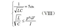
In order to avoid the ripple of the power supply appearing in the dangerous area, it is generally required that ω >>ωn 0, and ω 5ωn 0 = is taken in the project. At this time, at the point of ωn, the amplification factor of the LC circuit on the ripple is 25 / 24 =1.042, and the amplification part does not exceed 5%. In addition, according to the requirements of the chip, the voltage drop of u2 cannot be greater than the percentage p%, and the inequality (VI) is obtained:
![]()
![]()
Simplify to get inequality (VII)

and combine ω 5ωn 0 = and inequality (VII) to get equation group (VIII):
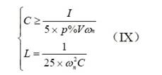
Solve until the inequality group (IX):
Since there is no ideal capacitor in reality, the actual capacitor has different filtering frequency bands, and the decoupling capacitor often uses a combination of capacitors with multiple capacitance values. C1 is the sum of the decoupling capacitor values. L is the sum of the inductance values.
2 π-type LC power filter circuit
2.1 π-type LC power filter circuit model and working principle
Since the front-end input power V provided by the power system is actually a variable value with many ripple components, when 0 0 <ωn < 2ω, the LC circuit has an amplifying effect on the ripple, so an improved version of the L-type LC filter circuit - the π-type LC power filter circuit (see Figure 2) is produced. Specifically, a filter capacitor is added to the front end of the inductor to form a π-type. In this way, the input power must first pass through a primary filter before entering the LC filter circuit, which can effectively improve the filtering effect of the LC filter circuit.
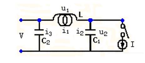
Figure 2 π-type LC power supply filter circuit
2.2 Analysis of the algorithm of π-type LC filter circuit
C2 should choose a suitable value. Choosing too large will increase the cost, and too small will affect the filtering effect. In practice, C2 = C1, which is similar to the second-order Butterworth filter. The characteristic of Butterworth filter is that the frequency response curve is the flattest in the passband and gradually decreases to 0 in the stopband, which can achieve better filtering effect.
3 LAYOUT design of LC filter circuit
LAYOUT is an important part of LC filter circuit. Reasonable LAYOUT can maximize the design effect, otherwise it will bring additional interference.
3.1 LAYOUT design of π-type LC filter circuit
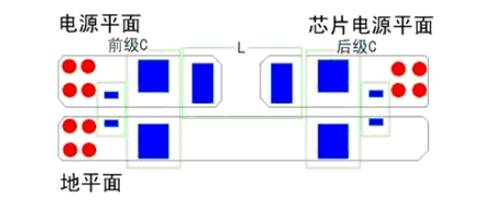
Figure 3: Layout effect diagram of π-type LC power filter circuit
The entire circuit is divided into three network planes: power plane, chip power plane and ground plane. In order to ensure the power connection effect and avoid causing additional voltage drop on the connected network, all networks are connected using copper foil. Taking the π-type LC filter circuit as an example, the effect of the entire circuit LAYOUT is shown in Figure 3. First, the power supply current is introduced from the power plane through the via hole. The power supply current enters the inductor after being filtered by the front-stage filter capacitor. After being choked by the inductor, the output current is output. The output current is filtered by the back-stage decoupling capacitor and then transmitted to the chip power plane through the via hole. When the power plane changes layers, more vias should be added to reduce the inductive reactance caused by the vias. In addition, the area where the power supply is obtained is adjacent to the area where the ground is obtained, which increases the accuracy of the level.
3.2 L-type LC filter circuit LAYOUT design
The L-type LC filter circuit LAYOUT design is similar to the π-type, except that the front-stage filter capacitor is missing and the power supply directly enters the inductor through the via hole for choking.
Conclusion
The algorithm and design of the LC power supply filter circuit for improving SSO proposed in this article have been found in practice that the LC filter has a significant inhibitory effect on medium and high frequency interference and can effectively improve the SSO problem. Its disadvantage is that it increases the number of components and brings costs. In addition, it is not applicable to circuits with particularly large current I because the corresponding inductance value is very small and difficult to achieve in production.
Previous article:Solutions for pressure sensors based on Wheatstone bridges
Next article:Application of atmospheric pressure sensor TP015P in altitude measurement
- Popular Resources
- Popular amplifiers
- High signal-to-noise ratio MEMS microphone drives artificial intelligence interaction
- Advantages of using a differential-to-single-ended RF amplifier in a transmit signal chain design
- ON Semiconductor CEO Appears at Munich Electronica Show and Launches Treo Platform
- ON Semiconductor Launches Industry-Leading Analog and Mixed-Signal Platform
- Analog Devices ADAQ7767-1 μModule DAQ Solution for Rapid Development of Precision Data Acquisition Systems Now Available at Mouser
- Domestic high-precision, high-speed ADC chips are on the rise
- Microcontrollers that combine Hi-Fi, intelligence and USB multi-channel features – ushering in a new era of digital audio
- Using capacitive PGA, Naxin Micro launches high-precision multi-channel 24/16-bit Δ-Σ ADC
- Fully Differential Amplifier Provides High Voltage, Low Noise Signals for Precision Data Acquisition Signal Chain
- Innolux's intelligent steer-by-wire solution makes cars smarter and safer
- 8051 MCU - Parity Check
- How to efficiently balance the sensitivity of tactile sensing interfaces
- What should I do if the servo motor shakes? What causes the servo motor to shake quickly?
- 【Brushless Motor】Analysis of three-phase BLDC motor and sharing of two popular development boards
- Midea Industrial Technology's subsidiaries Clou Electronics and Hekang New Energy jointly appeared at the Munich Battery Energy Storage Exhibition and Solar Energy Exhibition
- Guoxin Sichen | Application of ferroelectric memory PB85RS2MC in power battery management, with a capacity of 2M
- Analysis of common faults of frequency converter
- In a head-on competition with Qualcomm, what kind of cockpit products has Intel come up with?
- Dalian Rongke's all-vanadium liquid flow battery energy storage equipment industrialization project has entered the sprint stage before production
- Allegro MicroSystems Introduces Advanced Magnetic and Inductive Position Sensing Solutions at Electronica 2024
- Car key in the left hand, liveness detection radar in the right hand, UWB is imperative for cars!
- After a decade of rapid development, domestic CIS has entered the market
- Aegis Dagger Battery + Thor EM-i Super Hybrid, Geely New Energy has thrown out two "king bombs"
- A brief discussion on functional safety - fault, error, and failure
- In the smart car 2.0 cycle, these core industry chains are facing major opportunities!
- The United States and Japan are developing new batteries. CATL faces challenges? How should China's new energy battery industry respond?
- Murata launches high-precision 6-axis inertial sensor for automobiles
- Ford patents pre-charge alarm to help save costs and respond to emergencies
- New real-time microcontroller system from Texas Instruments enables smarter processing in automotive and industrial applications
- Advances in radar technology and the development of in-cockpit sensing technology
- Is it so difficult to post a message?
- [RVB2601 Creative Application Development] Ultrasonic pressure-sensitive buttons based on RISC-V processor
- First of all, the 9 boards sent by National Technology have arrived. It's so fast.
- There is no year-end bonus this year.
- Pingtou Ge RRVB2601 Review: Unboxing, Hardware Analysis and Environment Setup
- OrangePi Zero GPIO Control
- Play Basic with micro:bit
- PIC32MX250F128B please help?
- TI Cup 2019 National College Student Electronic Design Competition TI Processor Board Application Ten Questions and Answers

 LAYOUT_REPORT15-year summary of Taiwan\'s senior hardware engineer
 CVPR 2023 Paper Summary: Vision Applications and Systems


 京公网安备 11010802033920号