This application note is intended to help designers optimize the connection circuits between industrial sensors and high-performance ADCs in high-performance, multichannel data acquisition systems (DAS). Taking a power grid monitoring system as an example, this article explains the advantages of using the MAX11040 Σ-Δ ADC and how to select the appropriate architecture and peripheral components to optimize system performance.
introduction
In many high-end industrial applications, a high-performance data acquisition system (DAS) needs to provide appropriate interface circuits with various sensors. If the signal interface requires multi-channel, high-precision amplitude and phase information, these industrial applications can take advantage of the high dynamic range, simultaneous sampling, and multi-channel advantages of ADCs such as the MAX11040. This article introduces the MAX11040's Σ-Δ architecture and how to properly select the design architecture and external components to obtain the best system performance.
Advantages of High-Speed, Sigma-Delta Architecture
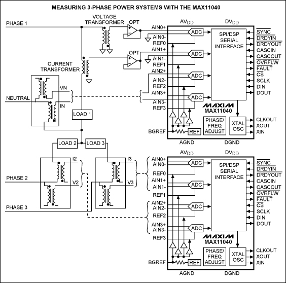
Figure 1 shows a high-end three-phase power line monitoring/measurement system. This type of industrial application requires accurate multi-channel simultaneous data acquisition with a dynamic range of up to 117dB and a sampling rate of 64ksps. In order to obtain the highest system accuracy, the signals from the sensors (for example, the CT and PT transformers in Figure 1) must be properly processed to meet the requirements of the ADC input range, thereby ensuring that the performance indicators of the DAS meet the requirements of relevant standards in different countries.

Figure 1. MAX11040-based DAS in power grid monitoring applications.
As shown in Figure 1, two MAX11040 ADCs can be used to simultaneously measure the voltage and current of the three phases and the neutral phase of the AC power. This ADC is based on a Σ-Δ architecture and uses oversampling/averaging to obtain higher resolution. Each ADC channel uses its own proprietary capacitor switch Σ-Δ modulator for analog-to-digital conversion. The modulator converts the input signal into a low-resolution digital signal, and its average value represents the quantized information of the input signal. The corresponding sampling rate is 3.072Msps when the clock frequency is 24.576MHz. The data stream is sent to the internal digital filter for processing to remove high-frequency noise. After processing, a resolution of up to 24 bits can be obtained.
The MAX11040 is a 4-channel simultaneous sampling ADC. Its output data is the average value after processing. These values cannot be regarded as the values of the sampling "instant" like the output of the successive approximation (SAR) ADC¹,².
The MAX11040 provides designers with many functions and features that are not available in SAR architectures, including: up to 117dB dynamic range at 1ksps sampling rate; integral nonlinearity and differential nonlinearity (INL, DNL) are also much better than SAR ADCs; unique sampling phase (sampling point) adjustment can internally compensate for phase offsets introduced by external circuits (drivers, transformers, input filters, etc.).
In addition, the MAX11040 integrates a digital lowpass filter to process the data stream generated by each modulator to obtain noise-free, high-resolution data output. This lowpass filter has a complex frequency response function, depending on the programmable output data rate. The resistor/capacitor (RC) filter at the input end combined with the MAX11040's digital lowpass filter greatly simplifies the design of the MAX11040 input signal path antialiasing filter, and can even completely eliminate the antialiasing filter. Table 1 lists some of the features of the MAX11040. For detailed information about the MAX11040 digital lowpass filter or the characteristics listed in the table, please refer to the device data sheet.
Table 1. Key specifications of the MAX11040 ADC
| Part | Channels | Input range (VP-P) | Resolution (Bits) | Speed (ksps, max) | SINAD (1ksps) (dB) | Input impedance |
| MAX11040 | 4 | ±2.2 | twenty four | 64 | 117 | High, (130kΩ, approx) |
ADC performance requirements for power line applications
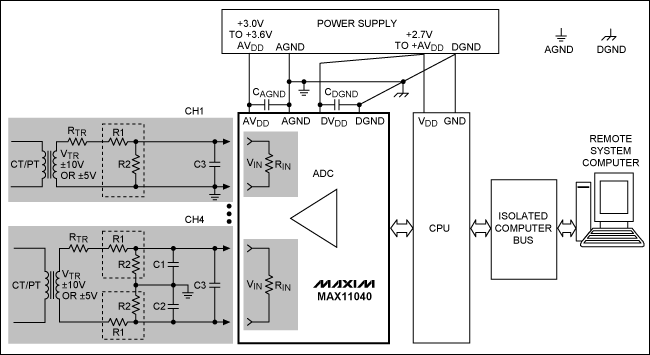
In power line monitoring applications, the output range of CT (current) transformers and PT (voltage) transformers is typically ±10V or ±5V peak-to-peak (VP-P). The input range of the MAX11040 is ±2.2VP-P, which is lower than the typical output of CT and PT transformers. However, a simple and low-cost solution can be used to adjust the ±5V or ±10V transformer output to the lower input range of the MAX11040, as shown in Figure 2.
The circuit connected to Channel 1 represents a single-ended design. In this configuration, one end of the transformer is grounded and the signal conditioning is accomplished using a simple resistor divider and capacitor.
For applications where common-mode noise (noise that has the same amplitude at both inputs of the ADC) is a concern, a differential connection circuit is recommended, as shown in Channel 4. The true differential inputs of the MAX11040 greatly reduce the impact of common-mode noise.

Figure 2. MAX11040 block diagram of a typical power line monitoring application, showing a transformer interface with ±10V or ±5V output. Channel 4 interface circuit is differential design, channel 1 is single-ended design.
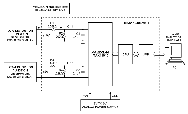
PT and CT measurement transformers are equivalent to low-impedance mutual inductors (equivalent impedance RTR is usually in the order of 10Ω to 100Ω). For ease of calculation, the following examples assume that the transformer is equivalent to a voltage source with an effective output resistance RTR = 50Ω; for demonstration purposes, the transformer can be replaced by a low-distortion function generator with 50Ω output impedance, as shown in Figure 3. The input impedance of the MAX11040 is related to the clock rate and the ADC input capacitance. Connecting appropriate bypass capacitor C3 and setting the XIN clock frequency = 24.576MHz, the input impedance RIN is equal to 130kΩ ±15%, and the error depends on the fluctuation of the internal input capacitance.
The resistor divider network composed of R1 and R2 converts the ±10V or ±5V input signal to the ±2.2V full-scale range (FSR) required by the ADC. To ensure that the circuit works properly, the values of R1 and R2 resistors and the selection of C1, C2, and C3 capacitors need to be optimized to meet the ±10V or ±5V input requirements. Resistors R1 and R2 must have high enough impedance to avoid overloading the CT and PT transformer outputs. At the same time, the value of R2 must be small enough to avoid affecting the input impedance of the ADC (R2 << RIN).
For a single-ended design, the input voltage VIN(f) of Channel 1 of the MAX11040 in Figure 2 can be calculated using Equation 1:

(Formula 1)
Where:
VTR is the output voltage of the CT and PT transformers.
RTR is the equivalent impedance of the transformer.
R1 and R2 form a resistor divider network.
RIN is the input impedance of the MAX11040.
R2llRIN is the parallel impedance of R2 and RIN.
C3 is the input bypass capacitor.
f is the input signal frequency.
VIN(f) is the input voltage of the MAX11040.
A similar approach can be used for differential input design.
To maintain a high-precision resistor divider ratio and proper bypass characteristics, metal film resistors with low temperature coefficients and 1% or better accuracy should be selected. Capacitors should be high-precision ceramic or film capacitors. It is best to purchase these components from reputable suppliers such as Panasonic®, Rohm®, Vishay®, Kemet®, and AVX®.
The MAX11040EVKIT provides a fully functional, 8-channel DAS system. The evaluation board can help designers accelerate product development, for example, to verify the recommended schematic solution in Figure 2.

Figure 3. Block diagram of a development system based on the MAX11040EVKIT. Two precision instruments are required to properly calibrate the measurement channels. The measurement results can be sent to a PC via USB and converted into an Excel® file for further processing.
The ±5V signal generated by a function generator is connected to Channel 2 of the MAX11040, while the ±10V signal generated by another function generator is connected to the input Channel 1 of the MAX11040. The resistor divider network R1/R2 and R3/R4 adjust the ±5V or ±10V input accordingly to make it close to the full-scale range of the ADC (FSR = ±2.2VP-P).
The values of the resistor divider network R1 and R2 and the bypass capacitors C1 and C2 are shown in Table 2 and are calculated by Equation 1 to approach the optimal input dynamic range (about ±2.10VP-P). This dynamic range is limited to a fairly high accuracy range of 0.05%, which is well suited for the MAX11040. For more information on accuracy specifications, refer to the MAX11040 data sheet.
Table 2. Resistor and bypass capacitor calculations for Figure 3.
|
VTR
±VP-P |
RTR
(Ω) |
R1
(Ω) |
R2
(Ω) |
RIN
(Ω) |
C3
(µF) |
f
(Hz) |
VIN
±VP-P |
VADC
(VRMS) |
Calibration
factor-KCAL |
Calibration
factor error (%) |
| Calculations for nominal VTR and standard components (nominal) values | ||||||||||
| 10 | 50 | 3320 | 909 | 130000 | 0.1 | 50 | 2.11268 | 1.4939 | 4.73301 | 0.70 |
| 5 | 50 | 2490 | 1820 | 130000 | 0.1 | 50 | 2.07026 | 1.46395 | 2.41516 | 0.99 |
| Measured values for VTR, VIN, VINRMS with real components values and tolerances used in the experiment | ||||||||||
| 9.863 | 50 ± 10% | 3320 ± 1% | 909 ± 1% | 130000 ± 15% | 0.1 ± 10% | 50 | 2.09872 | 1.483899 | 4.699912 | 0 |
| 4.932 | 50 ± 10% | 2490 ± 1% | 1820 ± 1% | 130000 ± 15% | 0.1 ± 10% | 50 | 2.06151 | 1.45833 | 2.3914 | 0 |
| 0 | 50 ± 10% | 2490 ± 1% | 1820 ± 1% | 130000 ± 15% | 0.1 ± 10% | 50 | 0 | 0.00048 | NA | NA |
The calculated values listed in Table 2 are derived from the results of Equation 1 and the precise measurements defined in Figure 3. The top of the table shows the theoretical calculation results of Equation 1 at the nominal input voltage, selecting standard discrete components. The bottom of Table 2 shows the actual measured component values and test errors in the demonstration system, as well as the KCAL coefficient used for FSR calibration and calculation, calculated as follows:
The calibration coefficient KCAL is calculated according to Equation 2:
KCAL = VTRMAX/(VADCMAX - VADC0) (Formula 2)
Where:
VTRMAX is the maximum input value, representing a ±5V or ±10V input signal, respectively.
VADCMAX is the measured, processed ADC value with the MAX11040 EV kit set up as shown in Figure 3, with the input signal set to VTRMAX.
VADC0 is the measured, processed ADC value with the MAX11040 EV kit set up as shown in Figure 3, with the input signal set to VIN = 0 (system zero offset measurement).
KCAL (in this case) is the calibration factor for that particular channel, calculated from the input signal VTR based on VADC.
The KCAL error calculation shows that the "theoretical" KCAL based only on the nominal value may differ by about 1% from the KCAL calculated based on the actual measured value.
Therefore, relying on theoretical calculations alone is not enough to support practical requirements; if the design needs to achieve the 0.2% accuracy required by the EU IEC 62053 standard, a full-scale range (FSR) calibration must be performed on each measurement channel.
The results shown in Table 3 verify the measurement of a ½ FSR input signal. The data was measured using a high-precision HP3458A multimeter, and the calibration coefficient KCAL in Equation 2 was used to obtain the ADC measurement and calculation values.
Table 3. Measurement results for verifying ½ FSR input signal
| Generator | Generator | MAX11040 | Calculation | Verr | Requirements |
| Nominal signal (½ FSR) | VTR_m - signal measured by HP3458A | VIN measured by ADC | VTR_C = VIN × KCAL | (VTR_M - VTR_C) × (100/VTR_C) | IEC 62053 |
| (VP-P) | (VRMS) | (VRMS) | (VRMS) | (%) | (%) |
| Channel 1: ±5.000 | 3.4892 | 0.74259 | 3.490126 | -0.026544 | 0.2 |
| Channel 2: ±2.500 | 1.7471 | 0.7307 | 1.747384 | -0.016265 | 0.2 |
In Table 3, VTR_M represents the measured value when the ½ FSR signal is input, while VTR_C represents the value calculated based on the MAX11040 measured value and KCAL processing.
The results show that the measured error VERR of the conditioned circuit is less than 0.03%, which can easily meet the 0.2% accuracy requirement of the EU IEC 62053 specification.

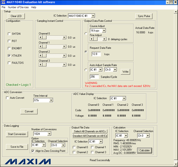
Figure 4. MAX11040EVKIT
The GUI allows the user to easily set various measurement conditions: 12.8ksps, 256 samples/cycle, and 1024 conversions. In addition, the calculation section of the GUI provides a convenient tool for quick engineering calculations.
The measurement results can also be transferred to the PC via the USB port, so that detailed data analysis can be performed using the powerful (and free) Excel.
in conclusion
High-performance, multichannel, simultaneous-sampling, sigma-delta ADCs such as the MAX11040 are ideal for data-acquisition systems in industrial applications. These new ADC designs offer up to 117dB of dynamic range, improved integral and differential nonlinearity, and sampling rates up to 64ksps. With the proper choice of signal conditioning, the MAX11040 can meet or exceed the specifications of advanced "smart" grid-monitoring systems¹.
Previous article:Implementation of low distortion, high precision adjustable sine wave generator
Next article:Brief analysis of LED ice and snow landscape lighting system design
Recommended ReadingLatest update time:2024-11-16 19:57


- Popular Resources
- Popular amplifiers
- High signal-to-noise ratio MEMS microphone drives artificial intelligence interaction
- Advantages of using a differential-to-single-ended RF amplifier in a transmit signal chain design
- ON Semiconductor CEO Appears at Munich Electronica Show and Launches Treo Platform
- ON Semiconductor Launches Industry-Leading Analog and Mixed-Signal Platform
- Analog Devices ADAQ7767-1 μModule DAQ Solution for Rapid Development of Precision Data Acquisition Systems Now Available at Mouser
- Domestic high-precision, high-speed ADC chips are on the rise
- Microcontrollers that combine Hi-Fi, intelligence and USB multi-channel features – ushering in a new era of digital audio
- Using capacitive PGA, Naxin Micro launches high-precision multi-channel 24/16-bit Δ-Σ ADC
- Fully Differential Amplifier Provides High Voltage, Low Noise Signals for Precision Data Acquisition Signal Chain
- Innolux's intelligent steer-by-wire solution makes cars smarter and safer
- 8051 MCU - Parity Check
- How to efficiently balance the sensitivity of tactile sensing interfaces
- What should I do if the servo motor shakes? What causes the servo motor to shake quickly?
- 【Brushless Motor】Analysis of three-phase BLDC motor and sharing of two popular development boards
- Midea Industrial Technology's subsidiaries Clou Electronics and Hekang New Energy jointly appeared at the Munich Battery Energy Storage Exhibition and Solar Energy Exhibition
- Guoxin Sichen | Application of ferroelectric memory PB85RS2MC in power battery management, with a capacity of 2M
- Analysis of common faults of frequency converter
- In a head-on competition with Qualcomm, what kind of cockpit products has Intel come up with?
- Dalian Rongke's all-vanadium liquid flow battery energy storage equipment industrialization project has entered the sprint stage before production
- Allegro MicroSystems Introduces Advanced Magnetic and Inductive Position Sensing Solutions at Electronica 2024
- Car key in the left hand, liveness detection radar in the right hand, UWB is imperative for cars!
- After a decade of rapid development, domestic CIS has entered the market
- Aegis Dagger Battery + Thor EM-i Super Hybrid, Geely New Energy has thrown out two "king bombs"
- A brief discussion on functional safety - fault, error, and failure
- In the smart car 2.0 cycle, these core industry chains are facing major opportunities!
- The United States and Japan are developing new batteries. CATL faces challenges? How should China's new energy battery industry respond?
- Murata launches high-precision 6-axis inertial sensor for automobiles
- Ford patents pre-charge alarm to help save costs and respond to emergencies
- New real-time microcontroller system from Texas Instruments enables smarter processing in automotive and industrial applications
- EEWorld interviews Toshiba PCIM booth engineer: 2-minute short video shows you key products and solutions
- Is it necessary to learn TI's KeystoneII series multi-core heterogeneous processors?
- cc2540 cc2541 low power consumption measurement and summary - and precautions - low power consumption less than 10uA
- Design of Serial Universal Asynchronous Receiver/Transmitter Based on FPGA
- Tesla Robot Optimus Prime Conference Uncut 4K HD Episode 2
- FPGA error, added clock timing, and how to solve this error
- [Project source code] FPGA-based Gigabit Ethernet module UDP design example program
- Here it comes! Summary of 2021 National College Entrance Examination Essay Questions
- Understanding IGBT Drivers in One Article
- A question of the direction of energy transmission

 ESP32-S3 source code
 【Follow me Season 2 Episode 2】Arduion UR4 homework submission code
 MCU C language programming and Proteus simulation technology (Xu Aijun)


 京公网安备 11010802033920号