FAQ: What factors should be considered when designing input drivers for 15Msps 18-bit ADCs
Introduction
ADC drivers are a key building block in data acquisition signal chain design. ADC drivers are used to perform many critical functions such as input signal amplitude scaling, single-ended to differential conversion, common-mode offset removal, and are often used to implement filtering. This Know-How and Comprehensive Knowledge (KWIK) Circuit Frequently Asked Questions (FAQ) note discusses how to generate a trimmed differential output signal from a single-ended input signal and level shift the signal to ensure that it meets the full-scale performance requirements of the ADC.
To help answer this frequently asked question, we will use the LTC6228, a low-noise, low-distortion, high-speed rail-to-rail output op amp, and the LTC2387-18 SAR ADC. We will use noise calculations to show the impact of the design on the overall SNR performance of the signal chain solution.

Figure 1. – Single-ended to differential conversion through trimming and level shifting
Design specification example
For this example, the design requirement specifications are shown in Table 1, and the input signal is a 0V to 5V sine wave. This design will use the ADC driver circuit shown in Figure 1 throughout. The function of this circuit is to convert, adjust, and shift the single-ended input signal into an appropriate differential output signal so that it can easily interface with the next stage in the signal chain (i.e., the ADC).
To analyze the performance of the circuit shown in Figure 1, we will use signal-to-noise ratio (SNR), taking the noise contribution of each stage and using it in the overall calculation. The SNR of the LTC2387-18 ADC and the spectral noise density of the LTC6228 used in the calculations are derived from the specifications in the corresponding data sheets.

Note that for this example, the effect of 1/f noise can be ignored because the target frequency is well above the 1/f region and the components selected (shown in Figure 1) are optimized to minimize noise contributions.
Design tips/notes
1. When choosing between single power supply and dual power supply, the following factors should be considered: Due to the margin requirements of the signal chain, single power supply may mean reduced signal swing, which may lead to reduced SNR; dual power supply must produce negative supply rail, adds complexity, but because the available headroom is increased, the signal swing can be higher and therefore the SNR performance is higher than the single-supply case. As can be seen from Table 1, we used an asymmetric supply of +7V/-3V. This supply voltage configuration provides enough headroom to ensure that the input and output ranges are maintained.
2.VBias is shown in Figure 1. This signal is used to convert the output signal level of the first stage to the common mode voltage level required to match the ADC input. As can be seen in Figure 1, this is accomplished simply by using a resistor divider, where the reference voltage Vref is used as the source.
Capacitor C5 is used to eliminate noise generated by the voltage divider.
Notice:
• The impedance of the driver network should be equal to the impedance of the feedback network. This is important when internal bias current cancellation is not available. This configuration will ensure that the additional offset voltage introduced by the bias current is reduced.
• If internal bias cancellation is used, high resistor values should be used to reduce power dissipation in this voltage divider network.
3. To reduce distortion errors, the RC filter should use high-quality capacitors (such as C0G (NP0)) and resistors.
4. Use a standard resistor value greater than the calculated value.
5. If power consumption is not a concern, the feedback resistor and gain resistor values of the two stages can be reduced to 301Ω to improve the SNR performance of the ADC and driver signal chain.
design steps
(Refer to Figure 1 for discussion)
• Signal conditioning and level shifting
• Solve for R1 using a transformation function

It should be noted that for low resistor values, the voltage noise of the LTC6228 dominates. As resistance increases, resistor noise begins to dominate. As the resistance continues to increase, current noise dominates.
If the resistor value of R2 is chosen to be 499Ω, the design can achieve a good balance between noise and power consumption.
Solve for R1

• Calculate VBias voltage value. This is done using the common mode voltage of Vi and Vo. The goal is to convert the output level of the first stage amplifier to 2.048V.
Vocm = 2.048V and Vicm = 2.5V
Then calculate Vbias as follows:

• Calculate the ratio to ensure the required bias voltage (Vbias) is achieved. Assume R8 = 499Ω to achieve balanced impedance at the input pin, then calculate R7. Noise from the voltage divider network is filtered out by C5

• Circuit noise analysis:
• First stage output - voltage noise calculation
The total voltage noise ( ) at the first stage output can be calculated using the following equation:

in:
– Voltage noise of op amp,
– Current noise* Noise due to source impedance
– Resistor noise
Calculate the noise gain of the first stage:

Solve for the voltage noise contribution due to current noise. According to the LTC6228 data sheet,
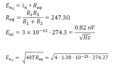

• Second stage output - voltage noise calculation
Use the same procedure to calculate the total voltage noise of the second stage  .
.
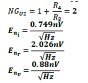
Using Equation 1 and the values calculated above, the second level is  :
:

• Noise bandwidth calculation
Calculate the effective noise bandwidth of each stage to convert voltage noise to rms noise.
Effective noise bandwidth of the first stage using a second-order filter
Use the following equation to solve for the effective noise bandwidth BWn. Here, k is the correction factor of the reference brick wall LPF, in this case it is 1.22, and n is the order of the filter.
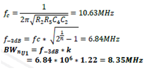
Second-stage effective noise bandwidth: third-order filter
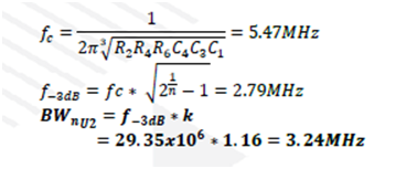
• Conversion of noise spectral density to rms noise
Convert the spectral density of each level into equivalent effective value noise.

Solve


Solve

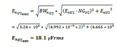
• Calculate total ADC driver noise
Calculate the total differential voltage noise of the ADC driver.

• ADC noise calculation
Solve for the ADC voltage noise for the full-scale input signal. Using 4.096Vp or 2.9Vrms, SNRadc = 95.7dB.
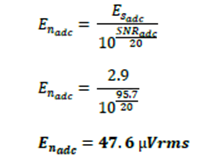
• Signal chain SNR calculation
Calculate the expected SNR performance based on the calculated ADC driver and ADC noise.
a. Full-scale input signal


b. -1.7dBFS input signal:
Where -1.7dBFS = 2.38VRMS

Design Simulation
The performance of the circuit in Figure 1 was simulated using the LTSpice simulation tool to determine whether the main target specifications were met.
The results obtained from the simulation test bench are shown in Figures 2-6
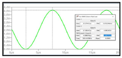
Figure 2. – Input Signal Adjustment
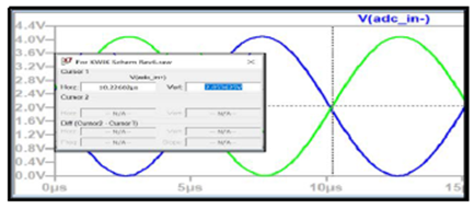
Figure 3. Output common mode voltage VOCM
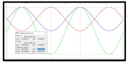
Figure 4: Differential output
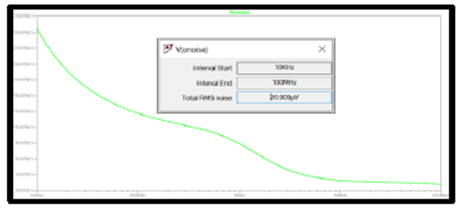
Figure 5 RMS differential noise
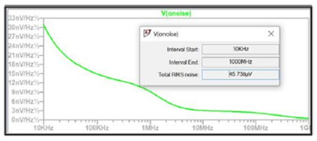
Figure 6. Total noise, ADC + driver

Measurement results
Obtain measurement results using the LTC6228 Evaluation Demonstration Board and the LTC2387-18 Evaluation Demonstration Board. For this example, the input signal is set to -1.7dBFS. The measured SNR for this signal chain is 92.13 dB. This result is approximately 1 dB lower than the calculated SNR (93.1 dB). The 1 dB difference is most likely due to non-ideal effects due to circuit board parasitics and tolerances of the components used. To achieve the expected full-scale SNR, increase the measurement by 1.7dB and the result will be 93.83dB, which is higher than the circuit design's target SNR performance.
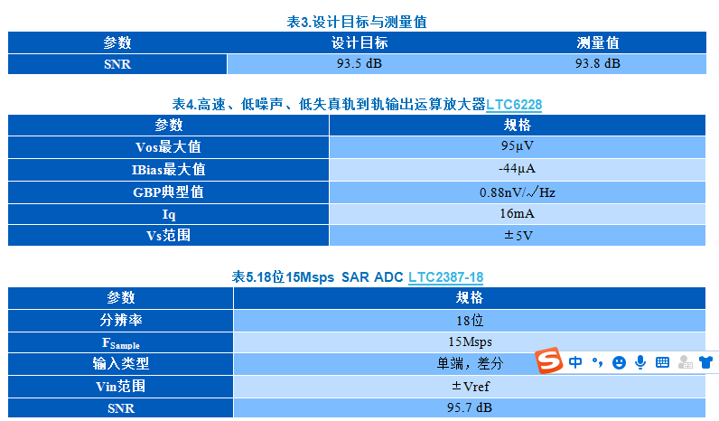
Design device
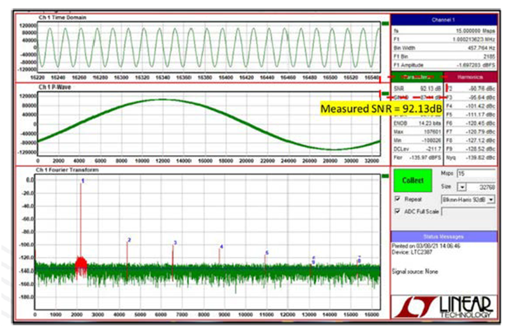
Figure 7 – Measured total SNR, ADC + driver
References
LTSPICE® is a high-performance SPICE III simulation software, schematic capture tool and waveform viewer that integrates enhanced features and models to simplify the simulation of switching regulators, linear regulators and signal chain circuits.
Analog Devices provides extensive technical guidance to establish the theoretical foundation. Here are some technical guides that have proven useful and worth reading to learn more.
MT-047 – Op Amp Noise
MT-048 – Op Amp Noise Relationships: 1/f Noise, RMS Noise, and Equivalent Noise Bandwidth
MT-049 – Operational Amplifier Total Output Noise Calculation for Single Pole Systems
MT-050 – Operational amplifier total output noise calculation for second-order systems
Previous article:Enhancing time-of-flight mass spectrometer performance with low-noise, high-speed ADCs
Next article:Analog Devices ADAQ7767-1 μModule DAQ Solution for Rapid Development of Precision Data Acquisition Systems Now Available at Mouser
- Popular Resources
- Popular amplifiers
- USB Type-C® and USB Power Delivery: Designed for extended power range and battery-powered systems
- ROHM develops the second generation of MUS-IC™ series audio DAC chips suitable for high-resolution audio playback
- ADALM2000 Experiment: Transformer-Coupled Amplifier
- High signal-to-noise ratio MEMS microphone drives artificial intelligence interaction
- Advantages of using a differential-to-single-ended RF amplifier in a transmit signal chain design
- ON Semiconductor CEO Appears at Munich Electronica Show and Launches Treo Platform
- ON Semiconductor Launches Industry-Leading Analog and Mixed-Signal Platform
- Analog Devices ADAQ7767-1 μModule DAQ Solution for Rapid Development of Precision Data Acquisition Systems Now Available at Mouser
- Domestic high-precision, high-speed ADC chips are on the rise
- Intel promotes AI with multi-dimensional efforts in technology, application, and ecology
- ChinaJoy Qualcomm Snapdragon Theme Pavilion takes you to experience the new changes in digital entertainment in the 5G era
- Infineon's latest generation IGBT technology platform enables precise control of speed and position
- Two test methods for LED lighting life
- Don't Let Lightning Induced Surges Scare You
- Application of brushless motor controller ML4425/4426
- Easy identification of LED power supply quality
- World's first integrated photovoltaic solar system completed in Israel
- Sliding window mean filter for avr microcontroller AD conversion
- What does call mean in the detailed explanation of ABB robot programming instructions?
- STMicroelectronics discloses its 2027-2028 financial model and path to achieve its 2030 goals
- 2024 China Automotive Charging and Battery Swapping Ecosystem Conference held in Taiyuan
- State-owned enterprises team up to invest in solid-state battery giant
- The evolution of electronic and electrical architecture is accelerating
- The first! National Automotive Chip Quality Inspection Center established
- BYD releases self-developed automotive chip using 4nm process, with a running score of up to 1.15 million
- GEODNET launches GEO-PULSE, a car GPS navigation device
- Should Chinese car companies develop their own high-computing chips?
- Infineon and Siemens combine embedded automotive software platform with microcontrollers to provide the necessary functions for next-generation SDVs
- Continental launches invisible biometric sensor display to monitor passengers' vital signs
- I have a question about the voltage regulator.
- GigaDevice GD32E231 DIY Competition Finalists
- Internal structure of MCS-51 microcontroller
- The live broadcast has ended [Microchip Embedded Security Solutions | RISC-V Safe Place]
- EEWORLD University Hall----Live Replay: Application of MSP430 in Stepper Motor
- Recruiting mbse part-time training teachers
- Introduction to the production method and equipment required for smart tag antennas (reposted)
- Application of Multi-function Oscilloscope in Frequency Converter Analysis and Measurement
- [NXP Rapid IoT Review] Data Cloud Synchronization
- I am offering a reward to find a DSP expert with sufficient skills to be my mentor. It will be paid.

 CDS-1402MM


 京公网安备 11010802033920号