Abstract: LDMOS RF power amplifiers dominate the GSM and CDMA base station markets due to their extremely high price/performance ratio. A key factor in ensuring high performance when using LDMOS amplifiers is to compensate the gate bias voltage to maintain a constant quiescent current as temperature changes. The Dallas Semiconductor DS1870 bias controller is one of many LDMOS RF power amplifier bias solutions currently available. This application note describes the implementation of an analog bias solution using the DS4303.

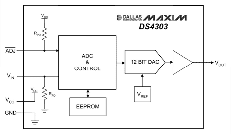
Figure 1. DS4303 functional block diagram
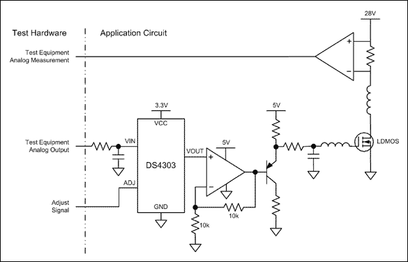
To calibrate the circuit, connect the required DS4303 output voltage to the VIN pin and adjust the signal to pull low to trigger the DS4303 to update the output voltage. Once the DS4303 has completed the update, the quiescent current is measured using a current sense amplifier; and the process is repeated until the appropriate bias voltage is reached. The input connected to the DS4303 must be kept stable to ensure that its output voltage reaches the correct value.

Figure 2. DS4303 LDMOS RF power amplifier bias circuit
Keywords:DS4303 LDMOS RF
Reference address:Using the DS4303 to Bias an LDMOS RF Power Amplifier
DS4303 Overview
The DS4303 (Figure 1) is a sample-and-hold voltage reference that accepts an analog input voltage and recovers that voltage at its output using a 12-bit digital-to-analog converter (DAC). Once the output has recovered the input voltage, the chip stores the output code in an EEPROM, generating a nonvolatile analog reference voltage. The output voltage is generated by an internal low temperature coefficient reference and buffered by a rail-to-rail op amp.
Figure 1. DS4303 functional block diagram
DS4303 LDMOS Bias Circuit
The circuit shown in Figure 2 can be used to temperature compensate the gate voltage of an LDMOS. The output voltage of the circuit is equal to the VOUT of the DS4303 multiplied by 2 plus the VBE of the PNP. The voltage of the DS4303 after doubling is a voltage source with a low temperature coefficient. The temperature coefficient of the VBE of the PNP tube is about +2mV/°C, which provides temperature compensation for the LDMOS. Assuming that the PNP tube and the LDMOS have a good thermal path, this circuit can provide good temperature compensation for the LDMOS.To calibrate the circuit, connect the required DS4303 output voltage to the VIN pin and adjust the signal to pull low to trigger the DS4303 to update the output voltage. Once the DS4303 has completed the update, the quiescent current is measured using a current sense amplifier; and the process is repeated until the appropriate bias voltage is reached. The input connected to the DS4303 must be kept stable to ensure that its output voltage reaches the correct value.

Figure 2. DS4303 LDMOS RF power amplifier bias circuit
Comparison of DS4303 Bias Circuit and DS1870 Solution
The main advantages of the DS4303 analog circuit solution are simplicity and low cost. If the circuit is placed close to the LDMOS, the good thermal path between the PNP tube and the LDMOS can make the gate voltage change correctly with temperature. Another advantage of this solution over the lookup table is that it is easy to program because the programming is for a single temperature bias point. This solution is fully analog after the initialization programming is completed, so once the system is calibrated, updating the lookup table will not cause output transients.
Previous article:Thermocouple Isolation Amplifier Circuit
Next article:The basic structure, main parameters and ideal characteristics of the amplifier
- Popular Resources
- Popular amplifiers
Recommended Content
Latest Analog Electronics Articles
- High signal-to-noise ratio MEMS microphone drives artificial intelligence interaction
- Advantages of using a differential-to-single-ended RF amplifier in a transmit signal chain design
- ON Semiconductor CEO Appears at Munich Electronica Show and Launches Treo Platform
- ON Semiconductor Launches Industry-Leading Analog and Mixed-Signal Platform
- Analog Devices ADAQ7767-1 μModule DAQ Solution for Rapid Development of Precision Data Acquisition Systems Now Available at Mouser
- Domestic high-precision, high-speed ADC chips are on the rise
- Microcontrollers that combine Hi-Fi, intelligence and USB multi-channel features – ushering in a new era of digital audio
- Using capacitive PGA, Naxin Micro launches high-precision multi-channel 24/16-bit Δ-Σ ADC
- Fully Differential Amplifier Provides High Voltage, Low Noise Signals for Precision Data Acquisition Signal Chain
MoreSelected Circuit Diagrams
MorePopular Articles
- LED chemical incompatibility test to see which chemicals LEDs can be used with
- Application of ARM9 hardware coprocessor on WinCE embedded motherboard
- What are the key points for selecting rotor flowmeter?
- LM317 high power charger circuit
- A brief analysis of Embest's application and development of embedded medical devices
- Single-phase RC protection circuit
- stm32 PVD programmable voltage monitor
- Introduction and measurement of edge trigger and level trigger of 51 single chip microcomputer
- Improved design of Linux system software shell protection technology
- What to do if the ABB robot protection device stops
MoreDaily News
- Huawei's Strategic Department Director Gai Gang: The cumulative installed base of open source Euler operating system exceeds 10 million sets
- Download from the Internet--ARM Getting Started Notes
- Learn ARM development(22)
- Learn ARM development(21)
- Learn ARM development(20)
- Learn ARM development(19)
- Learn ARM development(14)
- Learn ARM development(15)
- Analysis of the application of several common contact parts in high-voltage connectors of new energy vehicles
- Wiring harness durability test and contact voltage drop test method
Guess you like
- Sensors and measurement and control circuits
- Advanced usage of embedded C language
- A strange problem of TMS320F2812 caused by an eCAN bug
- [Evaluation of EVAL-M3-TS6-665PN development board] 2. Detailed explanation of functions
- A brief discussion on PCI_Express architecture.rar
- Free application: Allwinner heterogeneous multi-core AI intelligent vision V853 development board
- [Mill MYB-YT507 development board trial experience] Python displays memory and CPU real-time status 2
- I can't understand the circuit diagram at all
- [ESP32-Audio-Kit Audio Development Board Review] Part 2: ESP-ADF Pitfalls in the vs code Environment
- Infrared ToF technology will significantly improve the performance and reliability of proximity sensors

 TL072IYD


 京公网安备 11010802033920号