How to Use a High-Voltage, High-Current Driver Op Amp in a 4–20mA Current Loop
This article discusses how to use high-voltage, high-current drive op amps to convert voltage signals into ±20mA or 4–20mA current signals in process control industrial applications. Using the MAX9943 op amp as an example, experimental instructions and test results are given.
introduction
Current loops have a long history of use in process control industrial systems. Current loops can be used to convey information from remote sensors to central processing units, or from these central processing units to remote excitation sources. 4–20mA current loops are very common, but some systems use ±20mA current loops. For low-resistance loads, using high-voltage op amps to provide high current drive can eliminate external power FETs and simplify circuit design.
This article discusses how to use high-voltage, high-current drive op amps in 4–20mA current loops. The op amp converts the voltage signal from the DAC to a ±20mA or 4–20mA current output. The MAX9943 op amp was used in the experiment, and the test data is given in the article.
Current Loop Basics
A current loop typically includes a sensor, a transmitter, a receiver, and an ADC or microcontroller ( Figure 1 ). The sensor measures a physical parameter (such as pressure or temperature) and provides a corresponding output voltage; the transmitter converts the sensor output into a proportional 4mA to 20mA current signal; the receiver converts the 4–20mA current into a voltage signal, and the ADC or microcontroller converts the receiver's voltage output into a digital signal. 
Figure 1. Major components of a simple current loopIn
a current loop, information is transmitted via a current-modulated signal. For a 4–20mA system, 4mA typically represents zero output from the sensor, and 20mA represents full-scale output. It is easy to distinguish between an open loop (0mA, a fault condition) and zero output from the sensor (4mA).
Compared to voltage-modulated signals, current loops are inherently more immune to interference, making them ideal for noisy industrial environments. Signals can be transmitted over long distances, and information can be sent to or received from a remote location. Typically, the sensor is located far from the control center where the system microcontroller is located.
More complex systems include another current loop from the microcontroller or DSP to the excitation source ( Figure 2 ). The DAC converts the digital information into an analog voltage signal. The current loop transmitter converts the DAC output voltage into a 4–20mA or ±20mA current signal that drives the excitation source. Similar applications exist in power grid monitoring systems, which use sophisticated algorithms to determine the current state of the system, predict the direction of system change, and dynamically adjust the system through a control loop. 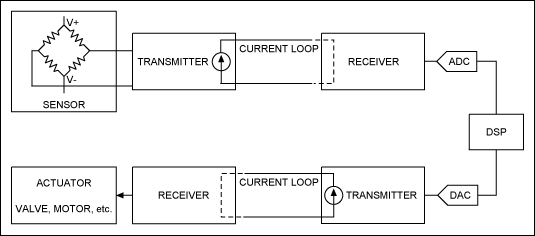
Figure 2. A complex system that uses another current loop to control the excitation source
Using operational amplifiers to achieve VI conversion and provide high current drive
The circuit shown in Figure 3 uses two op amps and a few external resistors to create a simple VI (voltage-to-current) converter. When powered by ±15V, the op amp (in this case, the MAX9943) can provide more than ±20mA of output current into a low-impedance load.
The MAX9943 is a 36V op amp with high-current output drive capability. It is stable when driving load capacitance up to 1nF. This device is ideal for industrial applications that need to convert the voltage signal of a DAC output into a proportional 4–20mA or ±20mA current signal. 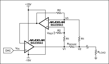
Figure 3. Using a VI converter to convert the DAC output to a load current, this circuit uses two MAX9943 op amps.
The relationship between the input voltage, V IN, and the load current is shown in Equation 1:
| V IN = (R2/R1) × R SENSE × R LOAD + V REF | (Formula 1) |
The component values in this circuit are:
R1 = 1kΩ
R2 = 10kΩ
R SENSE = 12.5Ω
R LOAD = 600ΩThe
typical load is in the hundreds of ohms. In the event of a short to ground fault or when the voltage load is reduced at the receiver for long-distance signal transmission, the load impedance will be significantly reduced.
V REF can use the same reference voltage as the DAC. In this case, all voltages (V IN ) are proportional to V REF , and errors due to V REF variations are eliminated .
Generate ±20mA Current Drive from ±2.5V
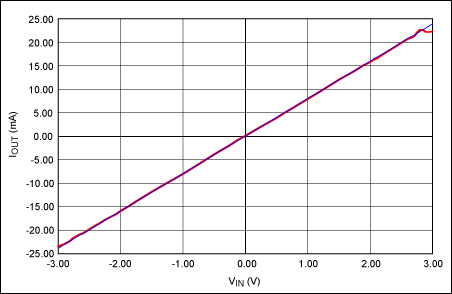
The circuit shown in Figure 3 can also be used to generate a ±20mA current drive. When V REF = 0V, an input range of -2.5V to +2.5V produces a nominal ±20mA current output, as shown in Figure 4. The relationship between
the input voltage (V IN ) and the “forward” op amp output voltage (V1) is as follows:
| V IN = (R2/R1) × (1 - α /β) × V1 + V REF × (1 - (R2/R1) × 1/(β × (R2 + R1))) | (Formula 2) |
Where:
| α = (1/R SENSE ) + R2/(R1 × (R1 + R2)) | (Formula 3) |
| β = 1/R SENSE + (1/R1) + 1/R LOAD | (Formula 4) |
Substituting the component values into Equation 2 and Equation 3:
| V1 = 4.876 × V IN - 4.872 × V REF | (Formula 5) |
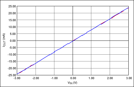
The relationship in Equation 5 helps avoid saturation of the output devices. In practice, the output of the lower op amp (V1) reaches approximately 12.2V when V IN = +2.5V. If the input voltage exceeds 2.5V, the output device eventually reaches its saturation point and the output voltage stops increasing. The curve in Figure 4 becomes flat, which is inconsistent with the ideal characteristic curve. Similar results occur when the inverting input is below -2.5V. Figure 4. ±2.5V input voltage range produces ±20mA output current. The blue curve is the ideal gain curve; the red curve is measured data. V CC = +15V; V EE = -15V. The data in Figure 4 shows that the MAX9943 can still operate in the linear range when the source and sink current reaches approximately ±21.5mA, which corresponds to ±2.68V input and the positive (lower) op amp output reaches ±13V. Because the output voltage of the MAX9943 can be very close to the negative supply voltage, the actual negative current can reach a large amplitude. The device's positive output swing is limited to within 2V of the positive supply voltage (the 2V value depends on the load and is a worst-case curve of technical specifications vs. process and temperature). Some applications require higher output current to meet design margin requirements or to leave some room for calibration. For such applications, the circuit in Figure 3 can be powered by ±18V dual supplies (instead of ±15V). In this case, the op amp can drive a maximum current of ±24mA (for ±3V input) and remain in the linear region, as shown in Figure 5. Figure 5. ±3V input voltage range produces ±24mA output current. The blue curve is the ideal gain curve; the red curve is measured data. V CC = +18V; V EE = -18V.
Generates 4–20mA current drive from 0 to 2.5V input range
From Equation 5 above, when V REF = -0.25V, the input range is from 0V to +2.5V and the current output can be 2mA to 22mA ( Figure 6 ). Often in a 4–20mA current loop, designers want some additional "headroom" in the dynamic range (for example, 2mA to 22mA) to allow for software calibration. If higher current is required, the MAX9943 can be powered from a ±18V dual supply, as described above. 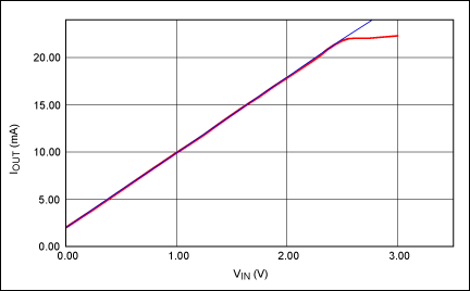
Figure 6. Generating 4–20mA output current from a 0V to 2.5V input voltage range. The blue curve is the ideal gain curve; the red curve is measured data. V CC = +15V; V EE = -15V.
in conclusion
Current loops are widely used in industrial applications that need to transmit information from remote sensors to central processing units, or from central units to remote excitation sources.
Experiments have shown that the MAX9943 op amp is well suited for control loop applications that convert voltage signals from sensors or DAC outputs into 4–20mA or ±20mA currents. The MAX9943 has high-current drive capability over the entire temperature range. It can maintain stable operation when driving capacitive loads up to 1nF, which are often encountered in long-distance transmission.
Previous article:Fiber Amplifier/EDFA, Principle and Classification of Fiber Amplifier/EDFA
Next article:Avago launches new high linearity power amplifier module products
- Popular Resources
- Popular amplifiers
-
 Evaluation and analysis of shift quality of passenger car dual-clutch transmission based on AVL-DRIVE system
 -
 A review of learning-based camera and lidar simulation methods for autonomous driving systems
 -
 Characteristic Modes——Theory and Applications in Antenna Engineering
 -
 Signal Integrity and Power Integrity Analysis (Eric Bogatin)
- High signal-to-noise ratio MEMS microphone drives artificial intelligence interaction
- Advantages of using a differential-to-single-ended RF amplifier in a transmit signal chain design
- ON Semiconductor CEO Appears at Munich Electronica Show and Launches Treo Platform
- ON Semiconductor Launches Industry-Leading Analog and Mixed-Signal Platform
- Analog Devices ADAQ7767-1 μModule DAQ Solution for Rapid Development of Precision Data Acquisition Systems Now Available at Mouser
- Domestic high-precision, high-speed ADC chips are on the rise
- Microcontrollers that combine Hi-Fi, intelligence and USB multi-channel features – ushering in a new era of digital audio
- Using capacitive PGA, Naxin Micro launches high-precision multi-channel 24/16-bit Δ-Σ ADC
- Fully Differential Amplifier Provides High Voltage, Low Noise Signals for Precision Data Acquisition Signal Chain
- Innolux's intelligent steer-by-wire solution makes cars smarter and safer
- 8051 MCU - Parity Check
- How to efficiently balance the sensitivity of tactile sensing interfaces
- What should I do if the servo motor shakes? What causes the servo motor to shake quickly?
- 【Brushless Motor】Analysis of three-phase BLDC motor and sharing of two popular development boards
- Midea Industrial Technology's subsidiaries Clou Electronics and Hekang New Energy jointly appeared at the Munich Battery Energy Storage Exhibition and Solar Energy Exhibition
- Guoxin Sichen | Application of ferroelectric memory PB85RS2MC in power battery management, with a capacity of 2M
- Analysis of common faults of frequency converter
- In a head-on competition with Qualcomm, what kind of cockpit products has Intel come up with?
- Dalian Rongke's all-vanadium liquid flow battery energy storage equipment industrialization project has entered the sprint stage before production
- Allegro MicroSystems Introduces Advanced Magnetic and Inductive Position Sensing Solutions at Electronica 2024
- Car key in the left hand, liveness detection radar in the right hand, UWB is imperative for cars!
- After a decade of rapid development, domestic CIS has entered the market
- Aegis Dagger Battery + Thor EM-i Super Hybrid, Geely New Energy has thrown out two "king bombs"
- A brief discussion on functional safety - fault, error, and failure
- In the smart car 2.0 cycle, these core industry chains are facing major opportunities!
- The United States and Japan are developing new batteries. CATL faces challenges? How should China's new energy battery industry respond?
- Murata launches high-precision 6-axis inertial sensor for automobiles
- Ford patents pre-charge alarm to help save costs and respond to emergencies
- New real-time microcontroller system from Texas Instruments enables smarter processing in automotive and industrial applications
- Digital Signal Processing (DSP) Library for MSP430 Microcontrollers
- LM5117 WEBENCH 13.6V-17.6V to 5.00V@3A Design Solution
- CCS6.0 creates a DSPc2000 series project operation steps
- Live FAQ: Renesas RA MCU family members are growing rapidly, helping to build safe and stable industrial control systems
- Bluetooth protocol analysis (5)_Technical analysis related to BLE broadcast communication
- [Voice and vision module based on ESP32S3] Software development progress - using openmvIDE, I can finally transfer pictures, the speed is...
- Check out the exclusive disassembly document! How do TWS earphones achieve hands-free and voice wake-up control?
- Shenmu Android Face Recognition SDK Compilation Instructions
- C6678 multi-core DSP development - several key issues of hello world
- For example, #35: #error directive "Not supported." What is the reason? Please give me some advice.

 Evaluation and analysis of shift quality of passenger car dual-clutch transmission based on AVL-DRIVE system


 京公网安备 11010802033920号