Overview
Electrodes are placed on both sides of the heart and close to the skin, and an electrocardiograph (ECG or EKG) records changes in the heart's electrical signals over time. The ECG displays the voltage difference between the electrode pairs, which represents the heart muscle activity. The heart rate signal is indicated on the display, making it easier for doctors to diagnose weak signals in different parts of the heart muscle.
The amplitude of the actual ECG signal is only a few millivolts, and the frequency does not exceed a few hundred hertz. ECG measurement faces many challenges: on the one hand, the 50Hz to 60Hz capacitive coupling interference from the ECG main power supply is much stronger than the useful signal; on the other hand, the contact impedance of the body skin and the impedance mismatch between sensors will cause large deviations and reduce the common mode rejection capability; in addition, the interference caused by contact noise and electromagnetic sources must be solved.
In most designs, an analog front end (AFE) is used to extract these signals, amplify and filter them, and then a 12-bit or 14-bit ADC is used for data acquisition. This article describes the main AFE components of an ECG system and provides a highly integrated design solution, the MAX11040K 24-bit simultaneous sampling Σ-Δ ADC. The MAX11040K provides the circuitry required for this application, eliminating the need for an AFE.
AFE Unit
The analog front end consists of three main components (Figure 1).
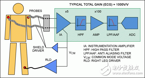
Figure 1. Typical ECG equipment typically uses an AFE for signal amplification and filtering, followed by an ADC for data acquisition.
1. Instrumentation Amplifier (IA)
The main task of the instrumentation amplifier (IA) is to reject common-mode signals (usually 50Hz/60Hz interference). ECG applications require a common-mode rejection ratio (CMRR) of 90dB or even higher to reject the 50Hz/60Hz signal coupled from the power supply before the amplification circuit. Even with an IA with a high common-mode rejection ratio (CMRR), the difference between different ECG electrodes or the mismatch between skin contact impedances not only produces offset drift, but also causes the CMRR to be lower than the desired level. Impedance mismatch mainly comes from the physical contact between the electrode and the skin, perspiration, and muscle movement.
The next factor to consider is the gain of the IA. When setting the IA gain, care must be taken to avoid excessive gain that causes clipping or saturation.
Also note that the audio signal is not in the same frequency band as the ECG signal. Therefore, typical audio amplifiers and Σ-Δ ADCs are not suitable for ECG applications because these devices have high input referred noise in the useful signal band.
The input impedance of the IA is also important because ECG measures weak signals. It is recommended to choose an IA with a high-impedance input because lower input impedance will result in greater signal attenuation.
2. High-pass filter
Although the initial signal is only in the mV range, it will rise to tens of millivolts after being amplified 5 or 10 times by the IA. And this level of signal can only cover a very small part of the ADC input range. For example, a 12-bit ADC has a ±4.096V input range and the least significant bit (LSB) is 2mV. If a signal of tens of millivolts is directly collected, there will not be enough resolution to distinguish between the signal and the sampling noise. Therefore, the signal needs to be amplified again, and the DC drift must be eliminated. The common AFE circuit uses a high-pass filter to feed back the unwanted signal (low-frequency interference) as a negative offset (negative feedback) to the IA input.
3. Second level amplification
After removing DC and low-frequency interference using the IA and high-pass filter, the second stage of amplification provides additional gain to reach the ADC input range. Some designs also add a notch filter to further suppress 50Hz/60Hz.
4. Low-pass/anti-aliasing filter
The low-pass filter is used to suppress high frequency interference. It also acts as an anti-aliasing filter (i.e., it blocks any signal greater than the Nyquist or 1/2 sampling frequency to avoid aliasing in the ADC).
To further reduce the input common-mode signal, ECG designs usually introduce a "right leg driver" to drive the inverted common-mode signal back to the human body. To ensure patient safety, an operational amplifier and a current-limiting resistor are usually used to ensure that a very weak signal source is driven into the human body. This shielding device is designed to reduce the noise coupling of the signal carried by the ECG probe.
In summary, the useful signal in ECG applications is less than 100mV, which is usually amplified to 2V considering offset and common-mode signals. Therefore, the AFE must have a 2V measurement range and can identify signals below hundreds or even tens of µV, with a sampling rate of around 1ksps.
The right ADC can reduce or even eliminate the need for an AFE
After the AFE design is completed, there are many ADCs that can meet the requirements of resolution, rate, and input range for actual applications. However, ADCs with high resolution, high common-mode rejection ratio (CMRR) and other advantages should still be given priority to ensure the design requirements of ECG.
The MAX11040K synchronous-sampling, Σ-Δ ADC alone exceeds the minimum requirements for such applications and can replace most of the system's functional circuitry, even eliminating the need for an AFE, providing a more reliable, smaller, and simpler design.
The MAX11040K has several essential specifications for application:
![]() Input range: ±2.2V
Input range: ±2.2V
![]() Differential input
Differential input
![]() 110dB common mode rejection ratio (typical)
110dB common mode rejection ratio (typical)
![]() 24-bit resolution:
24-bit resolution:
SNR >110dB
19-bit noise-free range
Effective resolution = 2/219 = 3.8µV
![]() ±6V input overvoltage protection
±6V input overvoltage protection
![]() Quad Fully Differential Simultaneous Sampling ADC
Quad Fully Differential Simultaneous Sampling ADC
Up to 32 channels can be cascaded for simultaneous sampling
![]() Programmable output data rate
Programmable output data rate
![]() Serial interface (convenient and safe isolation)
Serial interface (convenient and safe isolation)
![]() Programmable phase (sub-data rate)
Programmable phase (sub-data rate)
![]() Overvoltage/fault detection
Overvoltage/fault detection
Figure 2 shows a simple application of the MAX11040K. The differential input and 110dB common-mode rejection ratio can effectively suppress 50Hz/60Hz power-coupled noise. As a result, the MAX11040K can replace the first function of the IA. With its 24-bit resolution and 19-bit noise-free range, the MAX11040K has enough resolution to capture signal changes of a few µV. The first-stage amplifier (the second function of the IA), the second-stage amplifier, and the high-pass filter are eliminated. In addition, the device's ±2.2V input range is also very suitable for ECG applications.
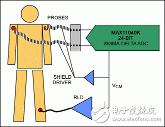
Figure 2. Using only the MAX11040K ADC to achieve the performance required for ECG applications reduces component count,
saves board space, and reduces overall system cost.
The MAX11040K has a sampling rate of 3.072MHz (oversampled Σ-Δ), but the output data rate (i.e., effective sampling rate) can be set from 64ksps to 250sps, increasing system flexibility. For small signals, the device has error smoothing capabilities, and the use of a Σ-Δ ADC architecture also eliminates the need for antialiasing filters. For a detailed introduction to Σ-Δ ADCs, refer to application note 1870, "Demystifying Σ-Δ ADCs."
Two other features of the MAX11040K are also very suitable for ECG applications, namely synchronous sampling and programmable phase delay. The 12-lead ECG is currently popular in the world, and it is very important to maintain the integrity of the phase. Each MAX11040K provides 4 differential channels, equivalent to 8 probes. The MAX11040K can cascade up to eight devices and support synchronous sampling of up to 64 channels. Not only can each channel be sampled simultaneously, but the phase of each channel can also be programmed (0 to 333µs delay, step size of 1.33µs).
We also offer a similar device with 16-bit resolution: MAX11046, which has ±6V input protection and generates an overvoltage fault alarm when the input signal exceeds 88% of the input range. A serial peripheral interface (SPI) reduces the requirement for optical isolators and eliminates the need for additional power supplies because its digital and analog supplies are separated.
Test Results for the MAX11046 Solution
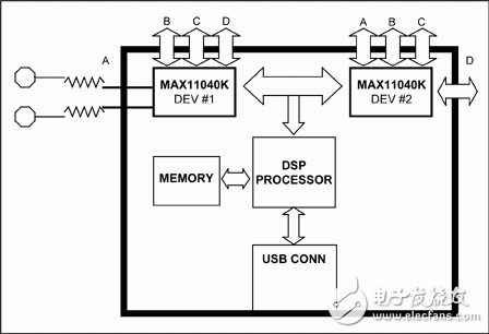
Figure 3. ECG application testing (using the MAX11040K EV kit).
Figure 3 is the block diagram of the MAX11040K evaluation board, which can be used for actual test evaluation. The evaluation board contains two MAX11040Ks, configured to work in 8-channel synchronous acquisition. The evaluation board can be plugged into the USB port of a PC and has memory and DSP, which is convenient for project development.
In the experiment, only copper foil was added to connect the ECG signal, and a 22kΩ resistor was connected in series between the ADC input and the electrode. The 130kΩ ADC input impedance (XIN clock frequency is 24.567MHz) caused the signal to attenuate by 75% (Figure 4). The test results are shown in Figure 5.
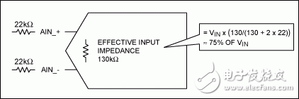
Figure 4. Equivalent input impedance of the MAX11040K.
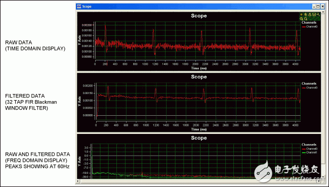
Figure 5. EKG data collection.
in conclusion
At the time of this article’s publication, the MAX11040K ADC is the only device on the market that meets the requirements for ECG measurements and provides ideal performance without increasing cost. The MAX11040K helps reduce your R&D budget, shortens design time, reduces board space, and reduces system component count, while also improving solution performance and reliability.
Previous article:Riverside: 3.3V input, 12V (15V) output isolated power supply
Next article:MAX2550-MAX2553 Transceiver Femtocell Wireless Reference Design
- Popular Resources
- Popular amplifiers
- High signal-to-noise ratio MEMS microphone drives artificial intelligence interaction
- Advantages of using a differential-to-single-ended RF amplifier in a transmit signal chain design
- ON Semiconductor CEO Appears at Munich Electronica Show and Launches Treo Platform
- ON Semiconductor Launches Industry-Leading Analog and Mixed-Signal Platform
- Analog Devices ADAQ7767-1 μModule DAQ Solution for Rapid Development of Precision Data Acquisition Systems Now Available at Mouser
- Domestic high-precision, high-speed ADC chips are on the rise
- Microcontrollers that combine Hi-Fi, intelligence and USB multi-channel features – ushering in a new era of digital audio
- Using capacitive PGA, Naxin Micro launches high-precision multi-channel 24/16-bit Δ-Σ ADC
- Fully Differential Amplifier Provides High Voltage, Low Noise Signals for Precision Data Acquisition Signal Chain
- LED chemical incompatibility test to see which chemicals LEDs can be used with
- Application of ARM9 hardware coprocessor on WinCE embedded motherboard
- What are the key points for selecting rotor flowmeter?
- LM317 high power charger circuit
- A brief analysis of Embest's application and development of embedded medical devices
- Single-phase RC protection circuit
- stm32 PVD programmable voltage monitor
- Introduction and measurement of edge trigger and level trigger of 51 single chip microcomputer
- Improved design of Linux system software shell protection technology
- What to do if the ABB robot protection device stops
- Keysight Technologies Helps Samsung Electronics Successfully Validate FiRa® 2.0 Safe Distance Measurement Test Case
- Innovation is not limited to Meizhi, Welling will appear at the 2024 China Home Appliance Technology Conference
- Innovation is not limited to Meizhi, Welling will appear at the 2024 China Home Appliance Technology Conference
- Huawei's Strategic Department Director Gai Gang: The cumulative installed base of open source Euler operating system exceeds 10 million sets
- Download from the Internet--ARM Getting Started Notes
- Learn ARM development(22)
- Learn ARM development(21)
- Learn ARM development(20)
- Learn ARM development(19)
- Learn ARM development(14)
- 【Child care machine】+ ESP32-S3-BOX+ESP32-S3-DevKitC-1 material unpacking and BOX basic demonstration
- [Free trial of Pingtouge Bluetooth Mesh Gateway Development Kit] + nRF Mesh and Light Experiment (Part 2)
- Allwinner V853 development board Tina SDK LCD small resolution DCLK setting problem
- Unboxing
- [TI star product limited time purchase] +CC2640R2
- What does the ratio difference in [ratio difference compensation] in the energy metering chip ATT7022 mean?
- How to choose resistors in circuit design?
- A time-delayed shutdown circuit
- Automotive 10V-80V Ultra-Wide Vin, 12V Vout Flyback Reference Design for 48V Car Battery
- TI Wireless MCU Offline Automatic Burning Instructions

 LV47002P


 京公网安备 11010802033920号