This paper mainly designs a relatively simple and universal wireless transceiver system based on the requirements of the 868MHz frequency band. The system can be applied to different wireless transmission applications in this frequency band.
SX1231 Introduction and Performance Description
The SX1231 chip is a highly integrated, low-power, multi-band UHF RF transceiver launched by Semtech. Its operating voltage is 1.8V~3.6V, 24-pin QFN package, and the operating frequency includes 3155MHz, 4335MHz, 8685MHz and 915MHz unlicensed ISM bands; it integrates SIGMA-DELTA fractional-frequency phase-locked loop, power amplifier, wake-up timer, digital modem, 66-byte transmit and receive data FIFO, data packet processing, data encryption function AES, and 6 configurable DIOs, etc. All major RF communication parameters are programmable, and most can be set dynamically. It uses a 16-section FIR channel filter, so it has good selectivity; the transmit power can be programmed from -18dBm to +17dBm; there are a variety of modulation and demodulation methods: FSK, GFSK, MSK, GMSK and OOK, etc.; SX1231 requires very few external components when in use, a 32MHz crystal oscillator, a few capacitors and inductors can form a high-reliability transceiver system, the design is simple and the cost is low. The sensitivity of SX1231 at 1.2kbps is as high as -120dBm, and it is mainly used in wireless meter reading (AMR), wireless sensor networks, home and building automation, wireless alarm and security systems, industrial monitoring and control, etc.
Wireless RF transceiver system design
System overall plan
The block diagram of the wireless RF transceiver system is shown in Figure 1. The STM8L151K2 microcontroller controls the SX1231 to realize the wireless data transmission and reception. The STM8L151K2 in the sending module transmits the data to the SX1231, and then the SX1231 processes the data in packet format, including adding a preamble, synchronization word, CRC check code, and encrypting the data if necessary. Finally, the data packet is sent to the receiving module via the antenna. After the receiving module amplifies, demodulates, and unpacks the received RF signal, it sends the data to the main controller STM8L151K2 for corresponding processing, such as sending it to the display screen or PC data processing center. The system includes human-machine interaction interfaces such as buttons and LCD screens, as well as RS232 interfaces, which realize the communication function with the PC.
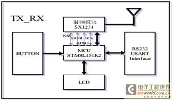
Figure 1 System block diagram
System hardware design
The main control chip is the single-chip microcomputer STM8L151K2 launched by ST. STM8L151K2 has 1K bytes of RAM, 8K bytes of Flash and 256 bytes of EEPROM. It integrates peripheral module interfaces including serial port, SPI, I2C, ADC, touch screen control function, etc., which fully meets the requirements of the system for microcontrollers; it has multiple power management modes (such as wait mode, low power operation mode, low power wait mode, etc.).
STM8L151K2 can read and write the internal registers of SX1231 through the SPI interface, and flexibly configure various parameters. Through the 4-wire SPI interface, the initialization configuration of SX1231, reading and writing data, accessing FIFO and other operations are completed, so that SX1231 can work normally in the transmission and receiving modes and complete the transmission of data in the air.
SX1231 is a standard SPI interface with 15~18 pins. DIO0~DIO5 can be configured as different interrupt signals through internal registers. The mapping relationship is shown in Table 1, which makes it easy to obtain the working status of SX1231. If you need to know the status of FIFO full, FIFO not completely empty, working mode Ready, valid data packet sending or receiving, low battery voltage, RSSI, PLL lock, etc., you can configure the register to map these signals to DIO PIN, and then the microcontroller STM8L151K2 obtains or actively notifies the MCU of a certain state by detecting the level of these DIO PIN. The 19th pin (RXTX) can be used to control the RF transceiver switch to switch the transmission path and the receiving path. The high level is the transmission state. UPG2214TB RF switch is used in Figure 2, and V1 and V2 are the control pins of the switch. Since SX1231 has only one control pin, adding a transistor inverter completes the control of the switch. Pin 21 (RFIO) is a common PIN for both transmission and reception, but the maximum output power of this PIN is 13dBm. If a higher output power (17dBm or 20dBm) is required, the transmission must be connected to pin 23 (PABOOST), and pin 21 (RFIO) is only used as a receiving PIN.
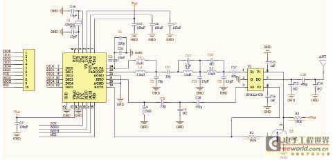
Figure 2 Hardware design schematic diagram
The input impedance of the SX1231 receiver can be set to 50Ω and 200Ω, usually set to 200Ω. At this time, the same matching value can still obtain good sensitivity in the full frequency band.
SX123 has some important features for saving power:
(1) Wide operating voltage range: It can work normally from 1.8V to 3.6V, and any characteristics remain unchanged. Especially for transmission, the output power is still the same when the operating voltage is as low as 1.8V, that is, the output power can reach 17dBm or 20dBm from 1.8V to 3.6V, and it does not change with the voltage. However, for other similar chips, the output power decreases as the voltage decreases. Such a feature enables the system to maximize the utilization of the battery and extend the battery life, which is of great significance for low-power applications.
(2) Registers can be read and written in sleep/standby mode: This feature saves power when writing to the FIFO. The current in sleep mode is 0.1μA, while the current in receive mode is 16mA, saving 160,000 times the power consumption.
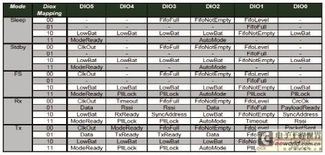
Table 1 DIO PIN and signal mapping table
System software design
Each major functional module in the system is compiled into an independent function and called by the main program. The functional modules include: initialization program (including initialization of STM8L151K2, SX1231), wireless transmission program, wireless reception program, etc. The wireless transmission program is responsible for writing the data payload to SX1231, and configuring the chip's preamble, synchronization word and CRC check code according to the communication protocol. Finally, SX1231 assembles it into a data packet and sends it out; the wireless reception program is responsible for receiving and processing data. First, SX1231 receives a complete data packet, then gradually removes the preamble, synchronization word and CRC code, and finally the MCU takes out the valid data from its FIFO.
The communication between wireless transceiver modules is sent in the form of data packets. The data packet format defined in this system is shown in Table 2.

Table 2 Data packet format defined in this system
Among them, the Preamble is a series of 10101010 (0XAA) or 01010101 (0X55), the number of which is 0~655635 bytes, and the specific number of bytes can be set according to the needs of the application. The preamble is mainly used for frame synchronization. The receiver mainly relies on the preamble to identify useful signals, complete frequency control, and automatic gain control, signal strength judgment and other actions to ensure that the correct data is received in the best state. SyncWord (synchronous word) is after the preamble. It is used as the flag code of the synchronization mode through the set synchronization word. It can also be used as a network ID. The devices in the same network use the same synchronization code. The following address code (Address) can be used as the ID of each device in the network. If the address in the data packet is the same as the address of this device, the data is received, otherwise it is not processed. The payload (Message) is the data that really needs to be transmitted. The last is the CRC check code, which is automatically completed by the chip.
Initialization Procedure
The initialization procedure includes the initialization of STM8L151K2 and the initialization configuration of SX1231's transceiver frequency, operating mode, modulation mode, data rate, and data packet processing registers.
After the system is powered on, the STM8L151K2 is in the default state and needs to be re-initialized and configured according to the system functional requirements. The SX1231 is also in the default state and needs to be configured before it can work. The initialization of the SX1231 is an important part, and the correct configuration has a great impact on the final communication performance of the system.
Data sending program
The wireless transmission program flow is shown in Figure 3. After completing the initialization of STM8L151K2 and SX1231, write the corresponding initialization RF control word into the configuration register; then write the data to be sent into the TX FIFO through the SPI continuous write register; then switch to the transmission mode. When the data is sent, the PacketSent register is set to 1, and the mapped DIO PIN will become a high level to notify the MCU that the data packet is sent. Then write the data to the FIFO and send it, and so on. Until all data is sent, enter the Sleep mode.
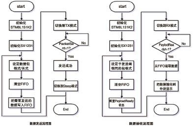
Figure 3 Data transmission and reception flow chart
Data receiving program
After the program completes the initialization of STM8L151K2 and SX1231, the corresponding initialization RF control word is written into the configuration register to configure SX1231 to receive state. When PayloadReady is detected as a high level, it indicates that data has been received, and then the MCU reads the data from the FIFO and processes it. This cycle continues until the reception is completed.
System test results
System test conditions and settings
This section is the settings for testing this system. According to different application requirements, some settings can be used for corresponding changes.
•Power supply voltage: 3.3V
• Frequency: 868.3MHz
• Data rate: 4.8kbps
• Frequency deviation: 5.0kHz
•Receiver bandwidth: 10kHz
•Data type: PN15
•Power setting: 4dBm
Test Results
Transmit power
As can be seen from Figure 4, the transmit power is 6.86dBm, which is lower than the regulatory requirement of 5mW (7dBm).
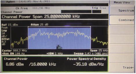
Figure 4 Transmitting power
Carrier frequency tolerance: 100x10-6
As can be seen from Figure 5, the output is set to 868.3MHz, and the actual measured frequency is 868.2960MHz. The frequency deviation is ((868.30-868.296)MHz/868MHz)=4.6×10-6, which is less than the specified carrier frequency tolerance of 100×10-6.
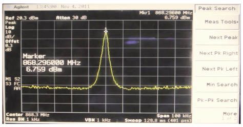
Figure 5 Carrier frequency tolerance
Transmit signal duty cycle limit: 1%
The duty cycle of the transmitted signal usually refers to the ratio of the time when the signal is transmitted to the time when the signal is not transmitted within a certain period of time. This mainly depends on the requirements of the application, but for short-distance wireless communication, the transmission time of the transmitter is very small, which is suitable for various control applications. For example, in the application of meter reading, the meter is read once a month, and the transmission time of each time is less than 1 second. This duty cycle is much less than 1%.
Previous article:Design of AOLONG Library Management System
Next article:Key Points of FPGA Application in Software Radio Design
Recommended ReadingLatest update time:2024-11-17 05:55


- Popular Resources
- Popular amplifiers
-
 Radio Frequency Identification (RFID) System Technology and Application (Written by Ci Xinxin, Wang Subin, and Wang Shuo)
 -
 Research on the relationship between load variables in microwave heating system based on radio frequency circuit
 -
 IoT Identification Technology
 -
 Basics of Machine Learning: From Getting Started to Job Hunting (Hu Huanwu)
- High signal-to-noise ratio MEMS microphone drives artificial intelligence interaction
- Advantages of using a differential-to-single-ended RF amplifier in a transmit signal chain design
- ON Semiconductor CEO Appears at Munich Electronica Show and Launches Treo Platform
- ON Semiconductor Launches Industry-Leading Analog and Mixed-Signal Platform
- Analog Devices ADAQ7767-1 μModule DAQ Solution for Rapid Development of Precision Data Acquisition Systems Now Available at Mouser
- Domestic high-precision, high-speed ADC chips are on the rise
- Microcontrollers that combine Hi-Fi, intelligence and USB multi-channel features – ushering in a new era of digital audio
- Using capacitive PGA, Naxin Micro launches high-precision multi-channel 24/16-bit Δ-Σ ADC
- Fully Differential Amplifier Provides High Voltage, Low Noise Signals for Precision Data Acquisition Signal Chain
- Innolux's intelligent steer-by-wire solution makes cars smarter and safer
- 8051 MCU - Parity Check
- How to efficiently balance the sensitivity of tactile sensing interfaces
- What should I do if the servo motor shakes? What causes the servo motor to shake quickly?
- 【Brushless Motor】Analysis of three-phase BLDC motor and sharing of two popular development boards
- Midea Industrial Technology's subsidiaries Clou Electronics and Hekang New Energy jointly appeared at the Munich Battery Energy Storage Exhibition and Solar Energy Exhibition
- Guoxin Sichen | Application of ferroelectric memory PB85RS2MC in power battery management, with a capacity of 2M
- Analysis of common faults of frequency converter
- In a head-on competition with Qualcomm, what kind of cockpit products has Intel come up with?
- Dalian Rongke's all-vanadium liquid flow battery energy storage equipment industrialization project has entered the sprint stage before production
- Allegro MicroSystems Introduces Advanced Magnetic and Inductive Position Sensing Solutions at Electronica 2024
- Car key in the left hand, liveness detection radar in the right hand, UWB is imperative for cars!
- After a decade of rapid development, domestic CIS has entered the market
- Aegis Dagger Battery + Thor EM-i Super Hybrid, Geely New Energy has thrown out two "king bombs"
- A brief discussion on functional safety - fault, error, and failure
- In the smart car 2.0 cycle, these core industry chains are facing major opportunities!
- Rambus Launches Industry's First HBM 4 Controller IP: What Are the Technical Details Behind It?
- The United States and Japan are developing new batteries. CATL faces challenges? How should China's new energy battery industry respond?
- Murata launches high-precision 6-axis inertial sensor for automobiles
- Ford patents pre-charge alarm to help save costs and respond to emergencies
- Sharing of key points on the use of ADI passive components
- Four design considerations for telematics hardware in connected cars
- Wide voltage input USB-C, 5V/3A output adapter reference design
- When the machine is turned off, the LDO output is normally 3V. Why does the voltage reach 3.5V after the machine is turned on? What is the reason?
- 【Smart Sports Watch】3. Build Development Environment 2
- History of the Development of Microwave Circuits
- 6657Statically configure serial port general interrupt in sys/bios
- C language binary division is represented by left and right shifts
- Understanding Nginx Architecture in One Article
- Highly recommended! ADI's latest Chinese information is here

 Radio Frequency Identification (RFID) System Technology and Application (Written by Ci Xinxin, Wang Subin, and Wang Shuo)


 京公网安备 11010802033920号