Improving accuracy has been a goal of vector network analyzer (VNA) measurements since the earliest days. VNA accuracy can be extended from the instrument port to the end of the test cable through calibration and vector error correction techniques. When the device under test (DUT) is directly connected to the test port cable, the calibration plane and the measurement plane are the same plane. In this case, calibration and error correction are a straightforward process involving mechanical or electronic coaxial calibration standards. However, for DUTs in pin-mount or surface-mount packages, test equipment must be used, and the coaxial calibration plane and measurement plane are currently separate, requiring additional error correction techniques to achieve high measurement accuracy. These methods often use modeled responses of the device to effectively move the correction plane to the port of the DUT. Some engineers choose to take the test equipment with minimal impact and simply measure the total response of the DUT and the device. This article discusses two model-based corrections that increase measurement accuracy and eliminate the need to ignore measurement errors introduced by the test equipment.
Direct measurement involves measuring the physical calibration standard and calculating the error terms. This approach provides high accuracy, primarily based on the degree to which the precise characteristics of the calibration standard are known. Many articles have been written over the years on the various direct measurement calibration techniques. All the details can be read in Agilent Application Notes 1287-3 and 1287-11. 1-3 Model-based calibration uses mathematical corrections derived from modeling the network response. This modeled response may come from simulation results or theoretical behavior, but is often derived from actual measurements. Often, a combination of measurement and modeling helps achieve the highest quality results.
Port extension, as shown in Figure 1, is the simplest modeling technique. It relies on a simple test device delay (and, in some cases, attenuation) model. De-embedding uses a complete S-parameter model of the device. Both techniques eliminate the need to build precise device internal calibration standards, which is difficult to achieve (especially for load standards) and takes a lot of time and effort.
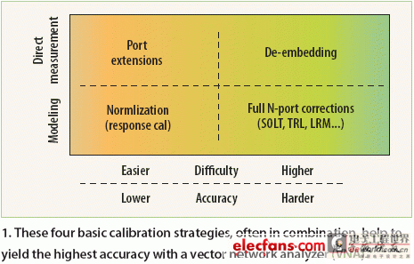
Test equipment varies widely, depending on the application and cost. While the test equipment used in manufacturing is rigorous and often expensive, printed circuit board (PCB) equipment in particular is common in research and development (R&D) labs. It is relatively cheap and easy to make, although signal losses at frequencies above 3 GHz cannot be ignored. Many devices in current wireless applications must be tested at frequencies up to 13 GHz. Therefore, it is necessary to reduce or eliminate the losses and delays of the device, so that the true characteristics of the DUT can be analyzed.
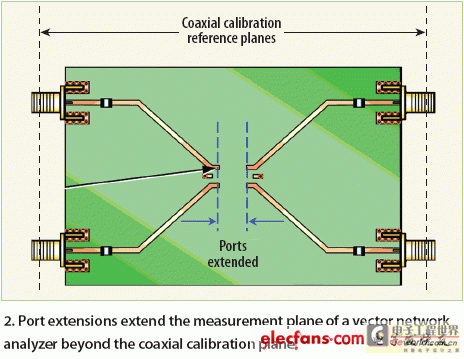
Therefore, when measuring the device in the fixture, the traces on the PCB are considered to be extensions of the coaxial test cable between the network analyzer and the DUT. By implementing port extensions on each piece of equipment, the measurement plane is extended beyond the coaxial calibration plane to the right to reach the port of the DUT. When the loss and electrical length between the device connector and the DUT are known, they can be subtracted manually by most VNAs available on the market.
Many test equipment uses PCB test equipment with SMA connectors (Figure 2). The test equipment/VNA combination can be calibrated at the SMA connector plane. However, when the test equipment is used to measure board mounted devices, the electrical characteristics of the PCB test equipment may change the measured amplitude and phase of the DUT. Port extensions are used to add linear phase (continuous delay) and loss vs. frequency terms to the coaxial error correction array that shifts the reference plane to the DUT plane.
When the delay and loss of a test device are unknown, they must be measured before port extension is used. Agilent Technologies has developed an automated method and integrated it into the PNA Series VNA. Agilent's Automatic Port Extension (APE) provides an easy way to calculate the loss and delay of a test device using a simple open or short circuit measurement. The electrical delay is calculated using the best-fit straight-line model. The loss terms are calculated using one of two methods, depending on the medium used for the transmission line. The loss model is assumed to be coaxial or dielectric. Both the coaxial and dielectric models provide a variable loss vs. frequency relationship that is not a simple straight line. The dielectric model is used when building the test device on a PCB.
The APE algorithm measures the open or short circuit and calculates the insertion loss and electrical delay of the tested portion of the test equipment. This step is repeated for each section of the test equipment. After this step, only the test equipment mismatch remains as a source of error. The main source of mismatch error is the transition from coaxial cable to microstrip line, which occurs at the connector of each test equipment port. This mismatch cannot be removed by coaxial calibration because it occurs after the coaxial calibration plane.
The measurement accuracy can be improved by using good quality edge-protruding connectors at the transitions to reduce reflections, and having good 50 ohm transmission lines in the test equipment. The port extension technique provides good results and has a moderate level of accuracy. Although not as accurate as using high quality in-equipment calibration standards, it is by far the easiest way to test devices in-equipment and provides sufficient accuracy for many applications.
The APE technique uses a curve fitting process to calculate low-order loss and phase responses. While the algorithm tolerates mismatched ripple, it does not remove the ripple itself. In most cases, only one highly reflective standard is needed to accurately calculate the loss and delay responses. Using only one highly reflective standard requires that the frequency range of the measurement be wide enough so that the ripple in the reflection measurement passes through at least one full cycle. In this case, the most convenient standard can be used, which is often an open circuit. Using two standards makes little difference for broadband measurements, since the standard or calculated loss that appears in the ripple is the same when an open or short circuit is used. Using two standards improves the accuracy of narrowband measurements, where a full ripple cycle does not occur. The lower trace shown in Figure 3 shows a portion of the test equipment response before APE is applied. The upper trace shows the response after APE is applied. Loss compensation may be centered around 0dB error (brown trace) or keep the ripple peak below 0dB (blue trace).
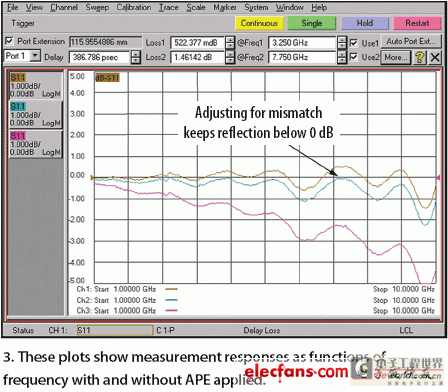
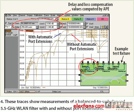
Figure 4 shows the response of a balanced to unbalanced 5.5 GHz wireless local area network (WLAN) filter tested to 10 GHz. The port delay and loss items for one of the test equipment are shown in the automatic port extension toolbar. The values are automatically calculated by the Agilent PNA network analyzer. The two traces below show the DUT measurement without port extension. Without port extension, the measurement includes both the DUT and the test equipment. The distorted response is due to the lack of phase compensation (especially important for balanced ports) and the lack of compensation for the losses of the transmission line on the PCB. With port extension, the severe errors due to the test equipment are removed and provide a fairly high degree of accuracy for the actual performance of the WLAN filter.
Test equipment de-embedding is a more rigorous modeling technique. The process begins by building a model of the test equipment used by the DUT. The accuracy of the model directly affects the accuracy of the de-embedded measurement. De-embedding is used to remove the undesirable effects of the test equipment, adapters, and probes. Instead of simply subtracting electrical length and insertion loss, de-embedding uses the modeled response as a function of frequency and mathematically removes the test equipment effects from the measurement. Unlike port extensions, de-embedding removes the effects of the mismatch of the coaxial to microstrip transition. The S-parameters of the test equipment circuit are stored in a .s2p file format.
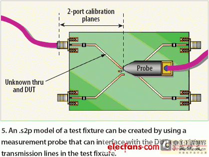
The simplest way to create a .s2p model of a test fixture is to use a measurement probe that interfaces with the DUT endpoint of the transmission line in the test fixture (Figure 5). In this case, the user implements an unknown through calibration using a coaxial standard on one side of the test fixture and uses a probe impedance standard substrate (ISS) on the other side of the test fixture. The transmission line of the test fixture is the unknown path. After calibration, the test fixture is simply measured without moving the probe or coaxial cable. The measurement process is repeated for each section of the test fixture, using the same calibration as the first fixture. In order to measure the transmission line endpoint with the probe, the ground plane must be placed on the test fixture with the correct spacing between the pitch of the test probe.
An alternative to probing the test equipment is to use a technique that implements two one-port calibrations. This technique assumes that the test equipment parts are interchangeable (i.e., S21 = S12), which is always the case. The first one-port calibration is performed at the end of the coaxial connector using a coaxial standard. The second one-port calibration is performed where the DUT is located using a calibration standard that is internal to the facility. Both the Agilent PNA and ENA network analyzers provide macros to extract the .s2p data for the test equipment parts, which use two sets of one-port calibration data. Although this method has the advantage of not requiring probes, it does require the generation and characterization of the calibration standards that are inside the test equipment in order to implement a one-port in-test equipment calibration.
If direct measurement of the test equipment is impractical, simulation can be performed to determine the S-parameter behavior of the test equipment portion. For accurate data based on this technique, a good loss model for the PCB material and accurate trace dimensions are required.
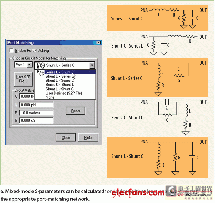
The exact opposite of test equipment de-embedding is test equipment embedding. If a network can be accurately subtracted from a measurement, it is reasonable that it can be easily added to the measurement. VNAs are matched to achieve S parameters in a 50 ohm single-ended environment. When the measurement device does not fit into this category, further processing of the data is required. Many of these software equipment tools are built into Agilent Technologies' PNA and ENA vector network analyzers. For non-50 ohm devices, it is possible to restate the S parameter data so that it looks like the DUT was measured using the VNA impedance, rather than 50 ohms. It is also possible to embed virtual impedance matching circuits, which is often required for devices such as surface acoustic wave (SAW) filters, without actually adding inductors and capacitors to the test equipment. Mixed mode (differential, common and cross mode) S parameters can be calculated for devices with at least one balanced port. Figure 6 shows some common impedance matching networks built into a VNA for this purpose.
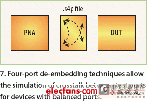
For devices with balanced ports, 4-port de-embedding allows crosstalk simulation between the test ports (Figure 7). Although crosstalk is negligible when using coaxial cables, it can become significant when test equipment or probes are used for measurement. Using two two-port .s2p files will provide different measurement results than using a single four-port file because the crosstalk terms are not included in the two-port file.
Port extension and de-embedding are important tools that should be added to every engineer's measurement toolkit to obtain the most accurate results. The PNA's automatic port extension feature guides the user through the required measurements to install by inference. In practical situations, test equipment de-embedding is recommended to obtain the most accurate measurement results. The PNA's calibration wizard easily implements the complete calibration procedure of probe de-embedding using a step-by-step guided process.
Previous article:Analyzing mobile phone wireless tests based on spectrum analyzer
Next article:The role of oscilloscope ENOB value in improving accuracy
- Popular Resources
- Popular amplifiers
-
 Evaluating Roadside Perception for Autonomous Vehicles: Insights from Field Testing
 -
 Signal Integrity and Power Integrity Analysis (Eric Bogatin)
 -
 Chip Manufacturing: A Practical Tutorial on Semiconductor Process Technology (Sixth Edition)
 -
 J1752™/3-SEP2017-Measurement of Radiated Emissions from Integrated Circuits—TEM/Wideband TEM (GTEM)
- High signal-to-noise ratio MEMS microphone drives artificial intelligence interaction
- Advantages of using a differential-to-single-ended RF amplifier in a transmit signal chain design
- ON Semiconductor CEO Appears at Munich Electronica Show and Launches Treo Platform
- ON Semiconductor Launches Industry-Leading Analog and Mixed-Signal Platform
- Analog Devices ADAQ7767-1 μModule DAQ Solution for Rapid Development of Precision Data Acquisition Systems Now Available at Mouser
- Domestic high-precision, high-speed ADC chips are on the rise
- Microcontrollers that combine Hi-Fi, intelligence and USB multi-channel features – ushering in a new era of digital audio
- Using capacitive PGA, Naxin Micro launches high-precision multi-channel 24/16-bit Δ-Σ ADC
- Fully Differential Amplifier Provides High Voltage, Low Noise Signals for Precision Data Acquisition Signal Chain
- Innolux's intelligent steer-by-wire solution makes cars smarter and safer
- 8051 MCU - Parity Check
- How to efficiently balance the sensitivity of tactile sensing interfaces
- What should I do if the servo motor shakes? What causes the servo motor to shake quickly?
- 【Brushless Motor】Analysis of three-phase BLDC motor and sharing of two popular development boards
- Midea Industrial Technology's subsidiaries Clou Electronics and Hekang New Energy jointly appeared at the Munich Battery Energy Storage Exhibition and Solar Energy Exhibition
- Guoxin Sichen | Application of ferroelectric memory PB85RS2MC in power battery management, with a capacity of 2M
- Analysis of common faults of frequency converter
- In a head-on competition with Qualcomm, what kind of cockpit products has Intel come up with?
- Dalian Rongke's all-vanadium liquid flow battery energy storage equipment industrialization project has entered the sprint stage before production
- Allegro MicroSystems Introduces Advanced Magnetic and Inductive Position Sensing Solutions at Electronica 2024
- Car key in the left hand, liveness detection radar in the right hand, UWB is imperative for cars!
- After a decade of rapid development, domestic CIS has entered the market
- Aegis Dagger Battery + Thor EM-i Super Hybrid, Geely New Energy has thrown out two "king bombs"
- A brief discussion on functional safety - fault, error, and failure
- In the smart car 2.0 cycle, these core industry chains are facing major opportunities!
- The United States and Japan are developing new batteries. CATL faces challenges? How should China's new energy battery industry respond?
- Murata launches high-precision 6-axis inertial sensor for automobiles
- Ford patents pre-charge alarm to help save costs and respond to emergencies
- New real-time microcontroller system from Texas Instruments enables smarter processing in automotive and industrial applications
- Fundamentals of RF/Microwave Switch Test System Design
- Bluetooth is down: BIAS attacks threaten all mainstream Bluetooth chips
- Will there be conflicts between Wi-Fi and Bluetooth in the same frequency band?
- Analog signal isolation GP9303+GP8101 solution
- A heating unit power supply solution with constant and adjustable output power based on TPS61022
- Who remembers a video about the principles of network communication?
- [Sipeed LicheeRV 86 Panel Review] 7 - lvgl Solution to the problem of incorrect image color display
- Wireless communication technology-NB-IoT
- SMT32 is no longer available, let's discuss alternative models
- Robotics (Stanford University Open Course)

 Evaluating Roadside Perception for Autonomous Vehicles: Insights from Field Testing


 京公网安备 11010802033920号