introduction
Initially, there was no standard for the digital communication interface for mixed-mode transmitters and network application processors (NCAPs) . Each transmitter manufacturer defined its own interface. Therefore, it was impossible for a transmitter manufacturer's products to support all control networks. To address this problem, the Sensor Technical Committee of the IEEE Instrumentation and Measurement Society launched an initiative to create smart transmitter interface standards for sensors, actuators, mixed-mode communication protocols, and the sensor electronic data sheet (TEDS) format. This initiative led to IEEE 1451.4-2004, which has been adopted as an American National Standard (ANSI).
The main objectives of this standard include:
Realize plug-and-play of sensors through public sensor communication interface.
Supports and simplifies the creation of smart transmitters.
Simplifies setup and maintenance of measurement instrumentation systems.
Enables deployment of smart transmitters with minimal memory capacity.
The standard states the following:
Transmitter, including Mixed Mode Interface (MMI) and Transmitter Electronic Data Sheet (TEDS).
MMI, used to access TEDS.
TEDS, a memory chip residing inside the transmitter.
Template illustrating the TEDS data structure.
Template Description Language (TDL).
A software object called a transmitter module accesses the TEDS through TDL and decodes and encodes it.
Transmitters that meet the IEEE 1451.4 standard can describe themselves via TEDS. This application note discusses the NCAP (data acquisition system) digital driver circuit for accessing TEDS.
IEEE 1451.4 Mixed Mode Interface (MMI)
The IEEE 1451.4 MMI is used to connect analog signals and TEDS between the transmitter and the NCAP or data acquisition system (DAS). The IEEE 1451.4 standard defines two classes of MMI. In Class 1, TEDS and analog functions share a single wire and use negative voltage communication. Class 2 provides TEDS communication on a separate wire pair and uses positive voltage communication. Therefore, Class 2 is consistent with Maxim's 1-Wire drivers (masters) as described in User Note 4206, "Choosing the Right 1-Wire® Master for Embedded Applications." Because Class 1 uses negative voltage communication, it requires a more complex driver circuit.
In Class 1, there are three MMI versions that use 2-wire, 3-wire, or 4-wire communication with a transmitter or TEDS. The commonality of these interfaces is that the analog and digital functions share a single wire. The shared wire can be a signal wire, a power wire, or a return channel.
Figure 1 shows a typical 2-wire constant current powered sensor with a common signal line. The diode allows sequential access to the amplifier or TEDS memory by reversing the polarity of the signal line. When the control switch is in the "analog" position, the positive current source of the DAS powers the amplifier through the signal line and the upper diode. The transmitter output appears as an analog voltage on the signal line. When the control switch is in the "digital" position, the memory device is powered by the negative logic supply through the lower diode. The circuit shows a pull-down resistor (Rt) between the terminals of the TEDS memory chip. This resistor is used to discharge the charge of the memory circuit and the lead capacitance to ensure that the logic 0 level meets the time slot requirements.
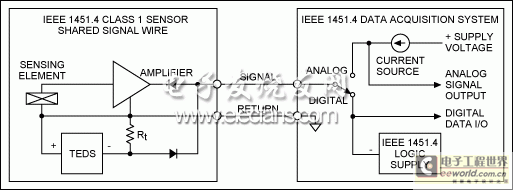
Figure 2 shows a block diagram of a 3-wire voltage-powered sensor with a common power line. The signal line is dedicated to delivering the analog output voltage of the transmitter to the DAS. The diodes allow sequential access to the amplifier or TEDS memory by reversing the polarity of the power line. When the control switch is in the "analog" position, the positive supply from the DAS power supply powers the amplifier through the upper diode. When the control switch is in the "digital" position, the memory device is powered by the negative logic supply through the lower diode.
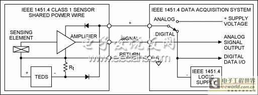
Figure 2. IEEE 1451.4 Class 1 MMI, shared power line.
Figure 3 adds another wire to create a 4-wire voltage powered sensor with a common return (usually a ground path) or shield. The sensor and TEDS memory have independent power supplies and can operate simultaneously. A switch to select analog and digital modes is still required to disable the digital function when the sensor is in use. This helps reduce the mutual interference noise between the analog signal and the digital TEDS data caused by the voltage drop in the common return. The diode and Rt are not required in this configuration. The resistor can be omitted and the diode can be replaced by a shorting line.
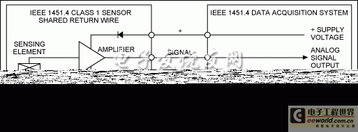
Figure 3. IEEE 1451.4 Class 1 MMI, shared return line.
TEDS Memory
The DS2430A 256-bit 1-Wire EEPROM is a typical TEDS memory chip. Since this chip has no VCC pin (i.e., it uses parasitic power), only two pins are required: IO and GND. The block diagram in Chapter 8.1.2 of the IEEE standard does not mention these pin names, but instead uses "+" to represent IO and "-" to represent GND. Figure 4 shows the digital portion of an IEEE 1451.4-compliant sensor, using the actual model number and pin names. The standard (Chapter 8.5, Family Code) does not specify a dedicated family code for TEDS memory. Therefore, it is allowed to use 2-pin 1-Wire memory chips other than the DS2430A. The general-purpose diode 1N4148 can be replaced by a Schottky diode, which has a forward bias voltage of approximately 0.3V. The Rt resistor value is not particularly critical, and the circuit was tested with 100kΩ.
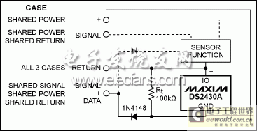
Figure 4. Class 1 sensor, TEDS operating principle.
Building a Class 1 MMI Digital Driver Circuit
The operating signal level of a 1-Wire device is 3V to 5V (pull-up voltage) in the idle state and 0V in the active state. This voltage is the voltage between the IO terminal (positive terminal) and the GND terminal (negative terminal). Class 1 MMI connects the IO pin to 0V and modulates the negative voltage of the memory chip's GND pin (Figure 5). Compared to the nominal 1-Wire signal level, the MMI signal is inverted and shifted 5V to the negative direction.

Figure 5. Nominal 1-Wire and Class 1 MMI signal levels.
The memory chip cannot distinguish and does not care how the voltage at its terminals is generated. When responding, it just applies a short-circuit signal to its port for a specified time. Under "normal conditions", this short-circuit signal is observed as a voltage close to 0V at the IO port. For Class 1 MMI, the short circuit causes the voltage on the digital communication line to rise from -5V (idle) to the diode drop -VF (-0.7V).
MMI Driver Description
Figure 6 shows the MMI driver circuit. The circuit consists of a forward path (top, master to sensor, write) and a return path (bottom, sensor to master, read). An IEEE 1451.4-compliant sensor is connected to TP4 through an analog/digital switch. The return path is connected to the driver's 0V (GND). The signal levels at TP2 and TP6 correspond to the nominal 1-Wire levels (5V for idle state and 0V for active signal level). V+ corresponds to the operating voltage of the microcontroller, which can range from 3V to 5V. TP2 is connected to an open-drain output (write) of the microcontroller, and TP6 is connected to an input port.
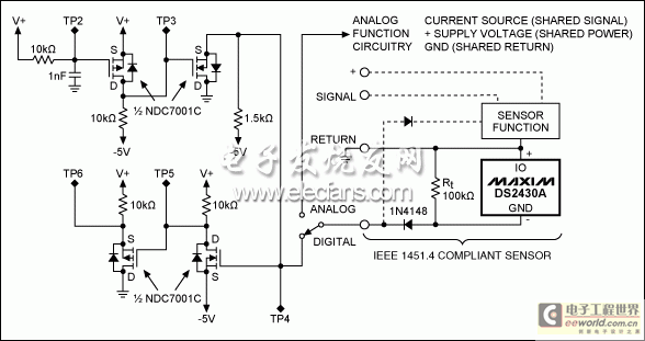
Figure 6. Class 1 MMI digital driver with sensor.
Connecting to a Bidirectional 1-Wire Master
Connecting a bidirectional master requires the additional circuit shown in Figure 7. Due to the different propagation delays for the rising and falling edges of the level-shifting section, the MMI driver using a bidirectional 1-Wire master may be unstable when the operating voltage is too high. For this reason, the positive supply needs to be limited to approximately 3.3V. Therefore, the bidirectional master must be a 3V powered device, such as the DS2482. Using a 5V bidirectional master (such as the DS2480B) will cause the COM and NO voltages of the analog switch to exceed the V+ level, which does not meet the required operating conditions.

Figure 7. Additional circuitry for bidirectional 1-Wire master interface.
verify
The circuit in Figure 6 was tested with the additional circuit in Figure 7. The 1-Wire master was the DS9097U-S09, which is based on the DS2480B driver chip. The positive voltage (V+) was set to 3.4V to ensure stability. The 1-Wire master operates at 5V, which does not meet the voltage requirements of the MAX4561 analog switch (signal voltage must not exceed the supply voltage). This explains the interference on TP2, but has no other adverse effects on the circuit's function.
Reset/Online Detection Cycle
Figure 8 shows the signals at TP2 (top), TP4 (middle), and TP6 (bottom). Due to the presence of diodes in the sensor network, the 0V level is not completely reached when the slave presence pulse is asserted. The bottom waveform shows a clear presence pulse. The positive amplitude at TP6 corresponds to V+ 3.4V.

Figure 8. Reset/online detection
Read time slot
The nodes shown in Figure 9 are the same as before (TP2 = top, TP4 = middle, TP6 = bottom). The first time slot reads 1 and the second time slot reads 0.
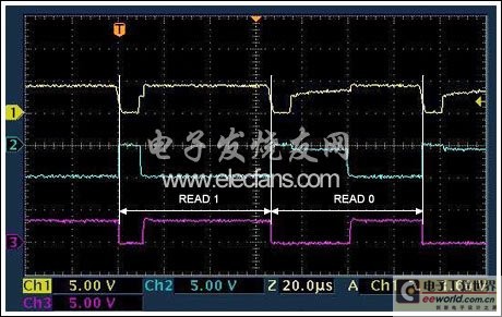
Figure 9. Communication time slots
Summarize
The circuits described in this article can be used when the microcontroller is acting as a 1-Wire master and using separate ports for read and write operations. However, the application software that generates the time slots and reset/presence detect signals has strict timing requirements and may have to be programmed in assembly language. The additional circuitry of the bidirectional 1-Wire driver chip allows the application software to be developed in a high-level language.
Due to its asynchronous operation, the add-on circuit can cause a spike when the master stops pulling the 1-Wire line low. When reading a 0, the spike triggers the driver's active pullup, causing a conflict between the driver's pullup and the MAX4561's pulldown. Therefore, when using the DS2482 driver, the active pullup should be turned off. The spike is also the reason why the bidirectional 1-Wire driver add-on circuit cannot support 1-Wire slaves on the master side.
Previous article:Methods for improving high-speed ADC clock signals
Next article:Bandgap Reference Calculator (BGRC) Function
Recommended ReadingLatest update time:2024-11-16 16:40
- Popular Resources
- Popular amplifiers
- High signal-to-noise ratio MEMS microphone drives artificial intelligence interaction
- Advantages of using a differential-to-single-ended RF amplifier in a transmit signal chain design
- ON Semiconductor CEO Appears at Munich Electronica Show and Launches Treo Platform
- ON Semiconductor Launches Industry-Leading Analog and Mixed-Signal Platform
- Analog Devices ADAQ7767-1 μModule DAQ Solution for Rapid Development of Precision Data Acquisition Systems Now Available at Mouser
- Domestic high-precision, high-speed ADC chips are on the rise
- Microcontrollers that combine Hi-Fi, intelligence and USB multi-channel features – ushering in a new era of digital audio
- Using capacitive PGA, Naxin Micro launches high-precision multi-channel 24/16-bit Δ-Σ ADC
- Fully Differential Amplifier Provides High Voltage, Low Noise Signals for Precision Data Acquisition Signal Chain
- Innolux's intelligent steer-by-wire solution makes cars smarter and safer
- 8051 MCU - Parity Check
- How to efficiently balance the sensitivity of tactile sensing interfaces
- What should I do if the servo motor shakes? What causes the servo motor to shake quickly?
- 【Brushless Motor】Analysis of three-phase BLDC motor and sharing of two popular development boards
- Midea Industrial Technology's subsidiaries Clou Electronics and Hekang New Energy jointly appeared at the Munich Battery Energy Storage Exhibition and Solar Energy Exhibition
- Guoxin Sichen | Application of ferroelectric memory PB85RS2MC in power battery management, with a capacity of 2M
- Analysis of common faults of frequency converter
- In a head-on competition with Qualcomm, what kind of cockpit products has Intel come up with?
- Dalian Rongke's all-vanadium liquid flow battery energy storage equipment industrialization project has entered the sprint stage before production
- Allegro MicroSystems Introduces Advanced Magnetic and Inductive Position Sensing Solutions at Electronica 2024
- Car key in the left hand, liveness detection radar in the right hand, UWB is imperative for cars!
- After a decade of rapid development, domestic CIS has entered the market
- Aegis Dagger Battery + Thor EM-i Super Hybrid, Geely New Energy has thrown out two "king bombs"
- A brief discussion on functional safety - fault, error, and failure
- In the smart car 2.0 cycle, these core industry chains are facing major opportunities!
- The United States and Japan are developing new batteries. CATL faces challenges? How should China's new energy battery industry respond?
- Murata launches high-precision 6-axis inertial sensor for automobiles
- Ford patents pre-charge alarm to help save costs and respond to emergencies
- New real-time microcontroller system from Texas Instruments enables smarter processing in automotive and industrial applications
- WiFi wireless changes: Goodbye 802.11, WiFi 4/5/6 is coming
- DIY Smart Timer
- 【Infineon XENSIV PAS CO2 Sensor】Sensor driver design
- MicroPython Hands-on (05) - Learn LCD screen with MaixPy from scratch
- MSP430 does not occupy IO to achieve a single-button power switch
- What are the categories of current sources? You will know after reading these
- Newcomer Registration
- How much do you know about how 5G mobile phones are designed to avoid radiation hazards?
- Questions about the PIOR register of Renesas MCU R7F0C004
- I have a LPV821 chip in my hand, and the teacher asked me to compare the package size

 Mission-oriented wireless communications for cooperative sensing in intelligent unmanned systems


 京公网安备 11010802033920号