1 Introduction
Currently, the mainstream video surveillance equipment on the market can be roughly divided into two categories. One is based on general-purpose microprocessors, and the other is based on digital signal processors (DSP). The two types of chips have their own functional characteristics. General-purpose chips are suitable for system control, management and information communication, while DSP chips are more suitable for performing complex digital calculations, audio and video data processing, etc. If the two chips work together, they can overcome their respective shortcomings to a certain extent and better utilize their advantages. Based on this consideration, this article proposes an interface design scheme between a general-purpose microprocessor (ARM) and DSP to achieve real-time communication between the two.
2 System Overview
2.1 Features of ARM7 S3C44B0X
S3C44B0X is a 16/32-bit RISC (Reduced Instruction Set Computer) architecture processor launched by SAMSUNG. It uses the ARM7TDMI core and the maximum operating frequency can reach 66MHz. This is a high-performance, low-power microprocessor that integrates a wealth of resources, including: 8KB Cache, RAM, LCD controller, DMA, UART and IIC bus interface, etc. Mainly used for the development of GPS positioning systems, wireless communications, handheld devices, monitoring systems and vehicle-mounted devices.
The S3C44B0X storage system supports 256MB of space, divided into 8 parts of 32MB each. System memory is allocated as BANK0~BANK7. Can be used to connect external memory and peripherals such as LCD and USB respectively. Among them, Bank0 is connected to FLASH and is used to store the system BIOS. Bank1 is connected to the FLASH hard disk and used as a system hard disk to build a file system. Bank2 is connected to the USB port, Bank3 is connected to the LCD module, Bank6 is connected to the SDRAM, and Bank4, Bank5, and Bank7 are reserved.
2.2 Features of DSP TMS20DM642
TMS320DM642 (DM642 for short) is the best-performing fixed-point DSP in the TMS320C6000 series. It is designed based on the Veloci TI second-generation high-performance very long instruction word VLIW (Very Long Instruction Word) architecture developed by Texas Instruments. The chip uses two The structure of level cache can support a series of powerful peripherals. DM642 has a large number of on-chip resources: 64-bit external memory interface, enhanced DMA controller, 16/32-bit HPI interface, IIC bus, GPIO, multimedia card controller, USB, multi-channel audio interface, 10/100Mbs Ethernet, management Data input and output modules, etc., it is a multimedia processor with superior performance and is the first choice for designing digital audio and video processing systems.
2.3 Introduction to host interface HPI
The HPI (Host-Post InterRFace) interface is a parallel communication port that connects the DSP and the host. It is an important interface for building a master-slave system and realizing communication between the host and the slave. The host can access all the storage space and address space mapped peripherals in the DSP through HPI, and then control the DSP to realize data exchange. The HPI interface of DM642 has two working modes: HPI16 and HPI32. In HPI16 mode, the high 16-bit data port HD[31:16] can also be used for PCI interface communication.
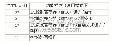
The HPI interface signal lines of DM642 include: 32 host data buses. In non-multiplexing mode, the data bus only transmits data signals, but in multiplexing mode, it can also be used to transmit address signals; HR/W_(_ means negative Logic valid) is the read/write signal enable of the HPI interface; HCS_, HDS1_, HDS2_ are chip select signals. The three are inside the DSP and pass through a logic gate as the read/write control logic of data; HRDY_ is ready Signal, when the output is low level, it means that the interface is busy, otherwise, it means that the interface can be operated; by controlling HRDY_, handshake communication between the host and the DSP can be realized; HINT_ is the interrupt request output of the DSP to the host; HHWL is used to High and low half words are recognized in 16-bit mode; HAS_ is the address strobe signal; HCNTL0/1 is the function selection bit of the HPI interface. The function description of HCNTL0/1 is as shown in Table 1.

Table 1 HCNTL0/1 function description
The HPI register occupies a total of 256KB of memory space, and the corresponding hexadecimal address range is: 0X01880000~0X018BFFFF. Among them, the starting address of HPIC is 0X01880000, the starting address of HPIA writing is 0X01880004, the starting address of HPIA reading is 0X01880008, and other address spaces are reserved. When the CPU reads and writes HPI, the HPI register must be set correctly.
3 Interface design
3.1 HPI interface read/write timing
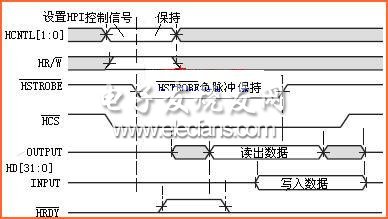
Read/write timing is an important point in realizing computer operations. If the operation timing does not match, it will cause errors in reading/writing data, or even operation failure. Therefore, meeting the operation timing is one of the prerequisites for computer operation. The DM642's HPI interface operation time is 1.3ns to 12ns or approximately 5 CPU clock pulses. The maximum clock frequency of S3C44B0X can reach 66MHz (approximately 15.2ns). It can be seen that the HPI of DM642 and S3C44B0X meet the read/write timing requirements, and interface communication can be achieved. The HPI32 read/write timing of DM642 is shown in Figure 1. This timing must be followed when designing the interface. As can be seen from the timing diagram, controlling the read/write timing of HPI can be achieved by controlling the signal ports HCNTL, HR/W_, HSTROBE_, HCS_ and HRDY_.

Figure 1 Read/write timing diagram of HPI32
3.2 Hardware design
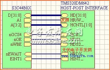
In this design, both S3C44B0X and DM642 are 32-bit processors, and DM642 has HPI32 mode. In order to make full use of resources and give full play to their advantages, the interface is designed in 32-bit mode. The hardware circuit is shown in Figure 2.

Figure 2 Hardware interface block circuit diagram
The connection instructions of each pin are as follows:
①HD[31:0] is connected to the data line D[31:0] of the CPU. In the multiplexing mode of the HPI interface, in addition to transmitting data, the 32 data lines HD[31:0] also need to transmit address signals.
②Chip select signal HCS_ is connected to nGCS4. The HPI interface is mapped to the reserved system memory BANK4, and the host can control HPI by operating BANK4.
③Since S3C44B0X does not have HR/W_ signal, it is replaced by A1 and connected to it. A2 and A3 are connected to HCNTL0/1 for interface function selection. nOE and nWBE are connected to HDS1_ and HDS2_ respectively as the read/write control signal input of HPI.
④nEWAIT connects to HRDY_. Since the effective logic levels of HRDY_ and nEWAIT of DM642 are opposite, they must be connected through a NOT gate. EINT1 is connected to HINT_, which is used by DSP to send interrupt requests to the host.
⑤In HPI32 mode, HHWL and address strobe signal HAS_ do not need to be used, and the pull-up resistor (high level) is fixed.
3.3 Software design
The host accesses the internal RAM of the DSP through the HPI interface, and reads/writes the RAM through the control register HPIC, address register HPIA, and data register HPID. The communication between the ARM host and the DSP slave is the operation of these registers. When writing the interface driver, the HPI interface is regarded as a peripheral connected to the host RAM. According to the hardware design, it is mapped to the storage space of BANK4 (the corresponding memory address is 0X08000000~0X0A000000).
Combining timing analysis and hardware design, interface drivers can be written. The driver mainly includes two parts: first, the HPI register initialization, and then the read/write code of the HPI interface. The following is part of the code for the HPI interface driver.
/* Address and data initialization*/
#define BASE_ADDR 0X08000000 //Define base address
/* Offset of HPIC, HPIA, HPID read and write addresses*/
#define HPIC_WR 0X00
#define HPID_A_WR 0X04
#define HPIA_WR 0X0C
#define HPIC_R 0X10
#define HPID_A_R 0X14
#define HPIA_R 0X1C
/*HPI reading and writing code*/
unsigned long hpi_read_data (unsigned long addr)
{ unsigned long data;
data=read_data(BASE_ADDR+HPID_R); // Read data
return(data); }
unsigned long hpi_write_data (unsigned long addr)
{ unsigned long data;
set_addr(addr); //Set the starting address
write_data(BASE_ADDR+HPID_WR); } // Write data
4 Conclusion
In the master-slave video surveillance system, high-speed communication between S3C44B0X and DM642 is realized through the design of HPI interface. The HPI read/write program running on S3C44B0X realizes access to the DM642 memory space by setting the corresponding interrupt control signal and operating the three registers HPIC, HPIA, and HPID, and can control data acquisition terminals and other data mapped to the memory space. peripherals, thereby realizing data exchange between dual cores. This proves that in the master-slave system constructed by S3C44B0X and DM642, the interface circuit designed by HPI can realize data communication between the two chips accurately and in real time.
Previous article:ARM and GPRS network constitute a home medical monitoring system
Next article:Industrial coal composition analysis system solution designed through S3C44B0X
Recommended ReadingLatest update time:2024-11-23 07:18


- Popular Resources
- Popular amplifiers
- Naxin Micro and Xinxian jointly launched the NS800RT series of real-time control MCUs
- How to learn embedded systems based on ARM platform
- Summary of jffs2_scan_eraseblock issues
- Application of SPCOMM Control in Serial Communication of Delphi7.0
- Using TComm component to realize serial communication in Delphi environment
- Bar chart code for embedded development practices
- Embedded Development Learning (10)
- Embedded Development Learning (8)
- Embedded Development Learning (6)
 Professor at Beihang University, dedicated to promoting microcontrollers and embedded systems for over 20 years.
- Intel promotes AI with multi-dimensional efforts in technology, application, and ecology
- ChinaJoy Qualcomm Snapdragon Theme Pavilion takes you to experience the new changes in digital entertainment in the 5G era
- Infineon's latest generation IGBT technology platform enables precise control of speed and position
- Two test methods for LED lighting life
- Don't Let Lightning Induced Surges Scare You
- Application of brushless motor controller ML4425/4426
- Easy identification of LED power supply quality
- World's first integrated photovoltaic solar system completed in Israel
- Sliding window mean filter for avr microcontroller AD conversion
- What does call mean in the detailed explanation of ABB robot programming instructions?
- STMicroelectronics discloses its 2027-2028 financial model and path to achieve its 2030 goals
- 2024 China Automotive Charging and Battery Swapping Ecosystem Conference held in Taiyuan
- State-owned enterprises team up to invest in solid-state battery giant
- The evolution of electronic and electrical architecture is accelerating
- The first! National Automotive Chip Quality Inspection Center established
- BYD releases self-developed automotive chip using 4nm process, with a running score of up to 1.15 million
- GEODNET launches GEO-PULSE, a car GPS navigation device
- Should Chinese car companies develop their own high-computing chips?
- Infineon and Siemens combine embedded automotive software platform with microcontrollers to provide the necessary functions for next-generation SDVs
- Continental launches invisible biometric sensor display to monitor passengers' vital signs
- Schematic diagram - What is the function of the enable pin of the PA chip?
- Friends who make power supplies, please take a look. TI chips can reduce the size of power supplies and charging time by half
- Shanghai Hangxin ACM32F070 Development Board + Touch Function Evaluation Board Evaluation - Part 3 Clock and Temperature Display Interface
- How to integrate electromagnetic compatibility (EMC) design into product development process
- [Silicon Labs Development Kit Review] + Driving the VEML6035 Ambient Light Sensor
- Development of Switching Power Supply for Deuterium Lamp
- [Ateli Development Board AT32F421 Review] + USART Development
- Integrated circuit technology lecture notes.
- What should I do if the USB is too long and there is a voltage drop?
- What do you think of my fingerprint lock?

 MATLAB and FPGA implementation of wireless communication


 京公网安备 11010802033920号