The reason for writing this article is that I found that there are few articles on the Internet that analyze the principles of STM32 registers. Maybe it is too simple and no one is willing to write. So I will write it down and try to make it simple and easy to understand, so as to leave a commemoration. It is definitely not well written or inaccurate in some places, please don't criticize it.
The power of the timer in STM32 is that you can not only use the internal clock and external pins to perform timing or counting like C51, but also use its own master-slave mode and capture/compare channels to perform more complex operations. For example, cascade multiple internal timers, capture or generate PWM waves, use the brake dead zone function, record the value of the encoder, etc. Some of these functions can be simulated by C51 through its IO pins, but some cannot.
Now let's get back to the topic. In combination with the newer HAL library, let's discuss the registers of STM32.
Let's talk about the CR1 register first. The manual starts with the CKD control bit:
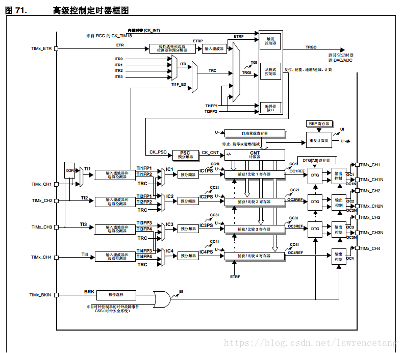
First post an important picture:
This picture is very important because it contains a lot of important information. From this picture, we can see that CK_INT is the internal clock, that is, the clock provided by the clock system of the microcontroller. Based on this clock, tDTS is obtained according to the configuration of this bit. The function of this clock is to determine the dead zone and sampling. This will be written when it is used.
Next, let’s look at the ARPE bit:
Because there is a concept of shadow register in the STM32 timer, the ARR register has a shadow register. The other two types of shadow registers are PSR and CCRX. We cannot directly operate this shadow register. In the end, it is this shadow register that has an effect on TIM. If this bit is configured to 1, we cannot directly update the shadow register when we update the value of the ARR register. We need to wait for the update event before we can put the value of the pre-loaded register into the shadow register. If it is configured to 0, when we update ARR, the automatic reload value of TIM will take effect immediately.
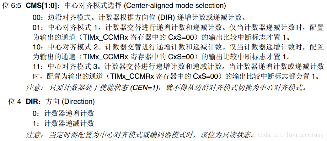
CMS bit and DIR bit configuration:
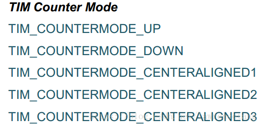
The manual explains this bit configuration clearly, how should it be configured in the hal library?
These parameters are used to configure this bit.
OPM bit configuration:
The manual gives an application example of single pulse mode as shown in the figure:
This figure is an example of TIM using the single pulse mode in PWM1 mode. The application of the single pulse mode is not limited to this, so it cannot be limited by this figure.
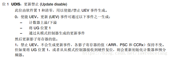
The configuration of this bit is relatively simple. It is used to configure and enable which events can become update events. After the update event occurs, if the corresponding interrupt is enabled, the flag of the interrupt will be set, and the interrupt program pointed to by the interrupt vector will be entered. The interrupt bit needs to be cleared in the interrupt program. If the corresponding DMA is configured, the DMA mode can be used to write the memory value to the various registers of TIM. This seems to be useless. DMA is generally used in peripherals with transmission communication properties, such as USART, USB, etc. In addition, the update event will also update the values of each shadow register and restart the counting of CNT.
Configuration of CEN bit:
If the SMS slave mode selection bit is not configured as gated mode or trigger mode, this bit is used to start and stop the timer. If gated mode or trigger mode is configured, the timer is started and stopped according to its trigger condition.
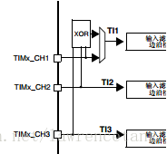
The CR1 register of TIM is finished, and the next is the CR2 register. Since the configuration of many registers has certain logical connections, they are not written in the order of registers. Let's talk about the configuration of TI1S bit first:
This is what it means. Since this is an XOR gate, after configuring it to 1, the input signal of TI1 is obtained by the XOR value of these three channels.
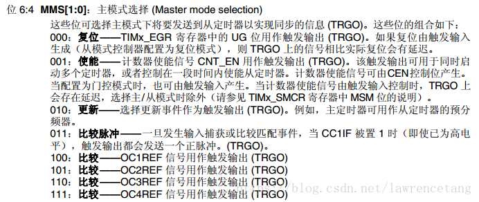
Configuration of MMS bit:
The above should be [2:0] instead of [1:0]. The configuration of this bit is very critical. It is what the master TIM needs to configure in the master-slave mode. To put it simply, these 8 configurations are about who will give the TRGO signal. The reset mode is given by the UG bit, the enable mode is given by the CEN bit, the update mode is given by the update event, and the comparison pulse mode is given when the CNT and CCRX comparison match occurs. The other modes are the reference levels of the four output channels. After the TRGO signal is output, if other TIMs are configured as slave mode, the signal can be used for the counting clock and trigger counting of the slave TIM. The relevant configuration needs to refer to the configuration of the SMS slave mode selection bit. Then look at the configuration of SMS:
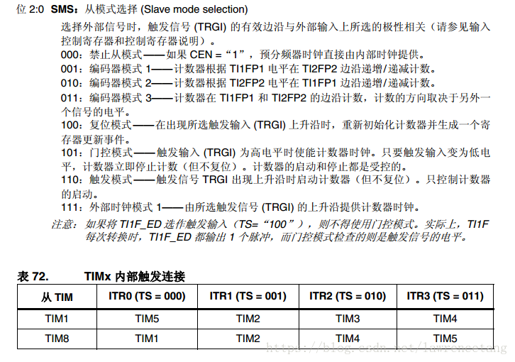
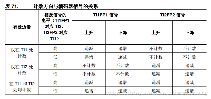
If you do not want to use the slave mode, you can directly configure it to disable the slave mode. This is the TIM counting only by the internal clock, and the trigger is by CEN. This mode of the encoder is quite useful, because the encoder has three items ABZ, connect the AB items to the TI1 and TI2 channels of the TIM, and then map IC1 to TI1 and IC2 to TI2 by configuring the CC1S and CC2S bits, and then configure the CC1P and CC2P bits to select the input polarity not to be reversed, so that the level entering the slave mode controller is the same as the level generated by the encoder. Finally, configure the slave mode to the encoder mode according to the level characteristics of the encoder output. There are 3 configuration modes as shown in the figure:
Finally, CEN is set to start counting. The encoders here refer to relative encoders.
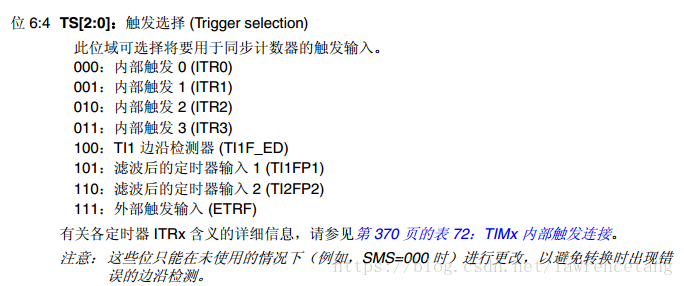
The reset mode is easier to understand. When TRGI has a rising edge, an event update is generated. The TRGI signal is generated by the TS bit configuration. If the TRGI in the reset mode is responsible for generating update events, then the gated mode and trigger mode are responsible for generating the start and stop timer, and the external clock mode 1 mode assigns the timer count. Their signals are all generated by the TS configuration. The configuration of the TS bit is shown in the figure:
The following configurations can be seen from the overall system diagram. The inputs of ITR0, ITR1, ITR2, and ITR3 should refer to the following table:
Since these are the contents of TIM1 and TIM8, only when these two TIMs are used as slave timers, the corresponding ITRX is connected to the TRGO of TIMX. For example, if the TS bit of TIM1 is configured as 000, the TRGO port of TIM5 is connected to the TRGI port of TIM1, and TRGO is determined by the MMS bit configuration mentioned above.
After talking about the master-slave mode, another important content of TIM is the application of input and output channels. This must start with the CCMR1 and CCMR2 registers.
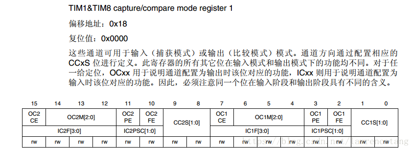
The CCMR1 register and CCMR2 register are similar, except that one is the configuration of channels 1 and 2 in TIM, and the other is the configuration of channels 3 and 4, as shown in the figure:
Obviously, the lower 8 bits are used to configure channel 1, and the upper 8 bits are used to configure channel 2. Taking channel 1 as an example, the first step is to configure the CC1S bit:
This bit indicates whether channel 1 is configured as input or output. Only one mode can be selected for configuration. Depending on this configuration, the meaning of the values of other bits of this register is also different.
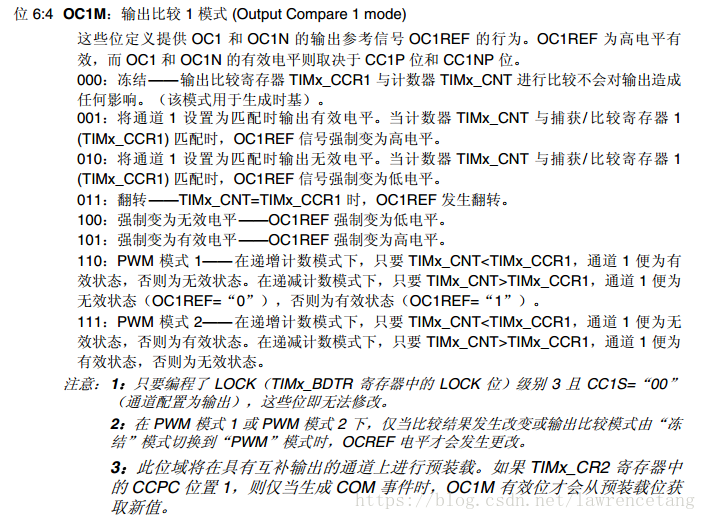
OK, let's assume that we configure it to output mode first, that is, CC1S bit is set to 00, then the configuration of other bits is the same as the one in the above row. What are they, 0C1CE, 0C1M, 0C1PE, 0C1FE, let's talk about the configuration of 0C1M bit first:
The first sentence of other manuals says that these bits define the behavior of the output reference signal OC1REF of OC1 and OC1N. That's right. It only defines the action of OC1REF. Why not directly define the action of OC1 and 0C1N? Because these two are the actual level outputs of the channel, it also depends on other related controls. Here we only need to know the level of 0C1REF. The definition of this level is fixed, that is, the effective state is high level, and the invalid state is low level. Here is another important picture:
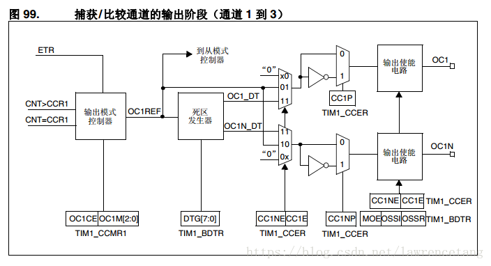
From this picture, we can see that OC1REF is controlled by 0C1CE and OC1M. OC1M can be configured to the above 8 modes. The core is that the TIM count value CNT and CCR value output different 0C1REF levels under different relationships. The rest is controlled by other registers. It can be said that different industry applications have different configurations for the following registers. Another one is the configuration of OC1CE:
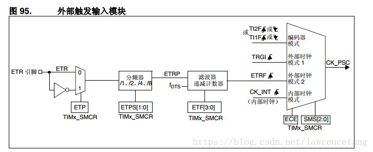
After configuring this bit, the level of OC1REF will be affected by ETRF. How does this ETRF come from? This starts with external clock mode 2:
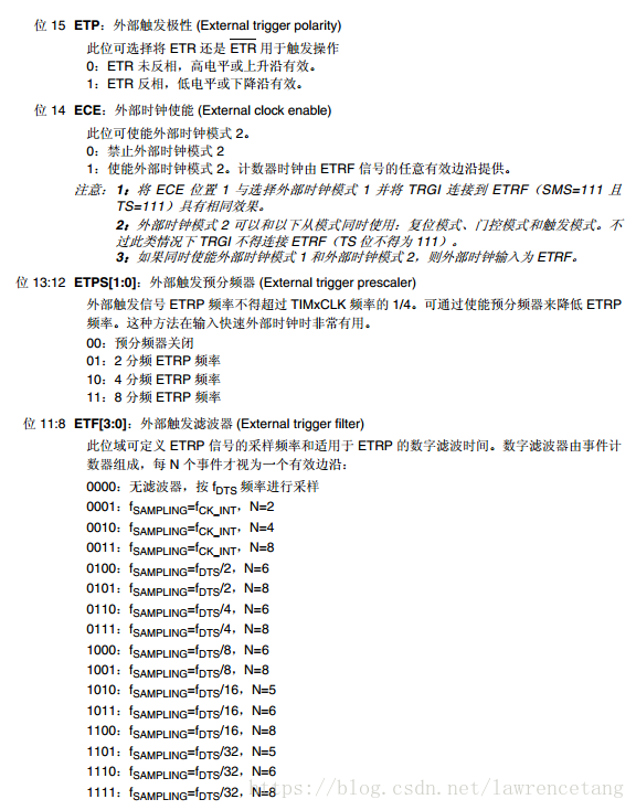
As can be seen from the figure, the control here is related to the SMCR register. This register is the slave mode register we mentioned at the beginning. Hahaha, let’s talk about the configuration of several bits together:
It is easy to understand from the diagram. The ETP bit is used to determine the effective edge, the ETPS bit is used to divide the external trigger signal, and the ETF bit is a filter configuration. The CKD bit we configured in the CR1 register at the beginning is useful here. The frequency of fDTS depends on the configuration of the CKD bit. What does fSAMPLING mean? For example, if it is configured to 1000, that is, Fsampling=Fdts/8, N=6, it means that the effective level of each external pulse must be maintained for at least 8 tDTS cycles to be considered a valid pulse. When 6 such pulses occur, it is considered a valid external pulse. The ECE bit enables external clock mode 2. Of course, ETRF can also be connected to external clock mode 1, provided that the slave mode is configured to external clock mode 1 and TS is to select external trigger input 111.
Next, let's talk about the output. There are two more bits of configuration, one is OC1PE and the other is OC1FE:
OC1PE is the configuration bit pre-loaded by CCR1. The concept of shadow register was mentioned earlier, and it is similar here.
I don't really understand the configuration of the OC1FE bit. I checked some information but couldn't find a good answer. According to the manual, it means fast output. Anyway, there is no problem in configuring it to 1 when using PWM output.
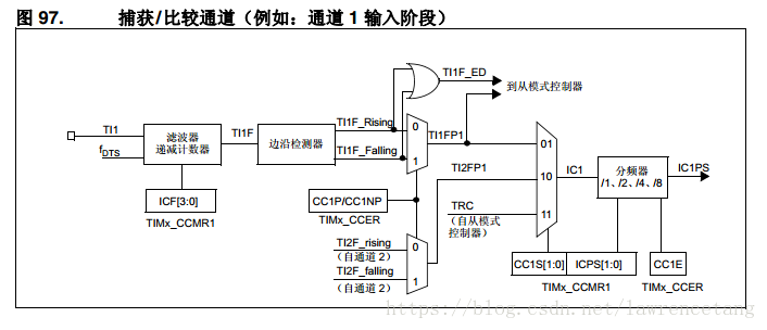
After the output, let's talk about the input. Here is a picture to help you understand:
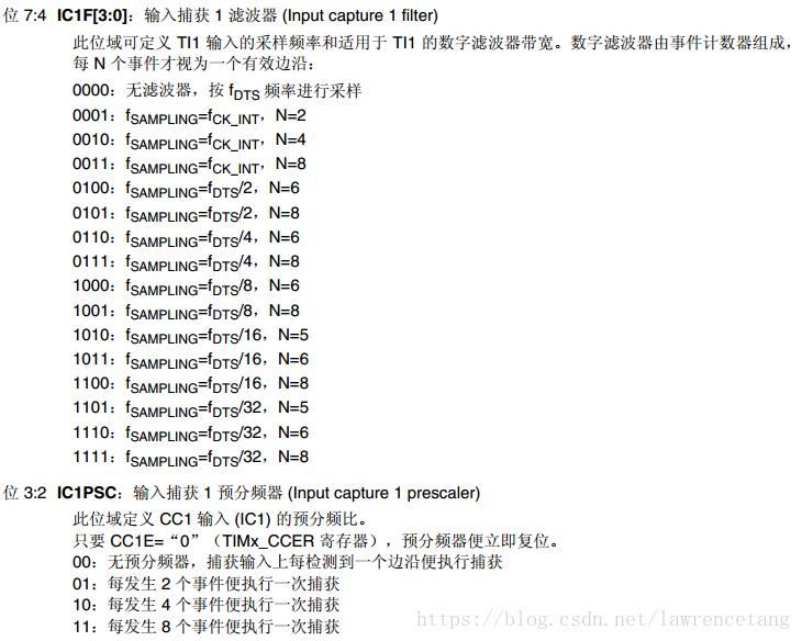
As expected, configure CC1S first. When this bit is configured as input mode, there are three options. In short, the signal of 01 is from its own channel TI1, the signal of 10 is from the adjacent 2 channels TI2, and the signal of 11 is from the slave mode signal TRC. The location of TRC can be clearly seen in the system diagram. Of course, the incoming signal must be processed, and the processing process depends on the configuration of the other bits. IC1F and IC1PSC in this register do this:
The input configuration is the same as that of ETR. You can understand it by following the same pattern. There is another bit configuration that also affects the effective level of the input, which is CC1P and CC1NP. This is what I will talk about soon.
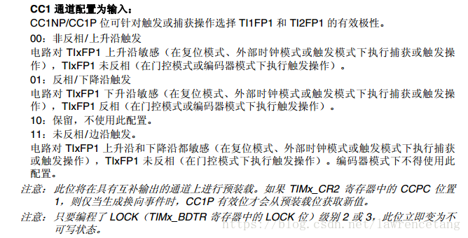
The configuration of these two bits still has different meanings when the channel is configured as input or output. I will take channel 1 as an example. I just talked about input, so I will first talk about the input configuration of these two bits. See the picture:
As can be seen from the figure, when the channel is configured as input, the effective level and polarity of the input signal are determined by the joint configuration of the CC1NP and CC1P bits in the CCER register, NP in front and P in the back. What I understand here is that when the input selected by TRGI is TI1FP1 and the slave mode is configured as reset, external clock 1, trigger mode, when configured as 00, the rising edge of the signal causes TRGI to generate a rising edge, when configured as 01, the falling edge of the signal causes TRGI to generate a rising edge, and when configured as 11, the rising and falling edges of the signal both cause TRGI to generate a rising edge. When the slave mode is configured as gated or encoder mode, configuring 00 or 01 only plays a positive and negative role in the signal.
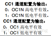
After saying this, let's talk about the functions of these two bits when channel 1 is configured as output:
I feel that the manual is ambiguous about it. Let's take a look at the output picture first. Obviously, the configuration of these two bits only plays the role of a NOT gate for the output signal, that is, when configured to 1, the OC1REF signal is logically NOT. We know that the effective level of OC1REF is a high level, so when configured to 1, when OC1REF is valid, the output is a low level, otherwise it is a high level. Of course, this is not the last hurdle for the output of OC1 and OC1N. The last one to control its level is the output enable circuit. Let's first introduce the CC1E and CC1NE bits of the CCER register:
Obviously, these two bits are used to enable the input or output channel. It seems simple, but there is a little mystery. Because the meaning of these two bits depends on some other configurations, the first of which is the configuration of the MOE bit, in the BDTR register:
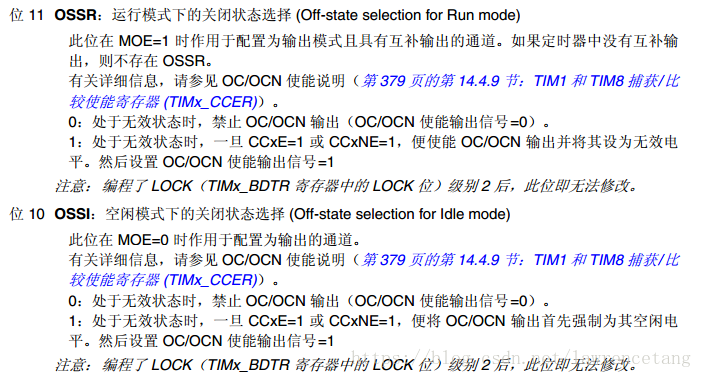
So, if you want OC and OCN to output normally, this bit must be 1. Then what is the effect when this bit is 0? The key point is that the two output channels will be forced to idle state. What is idle state? Let's look at the configuration of OSSR and OSSI. I means idle:
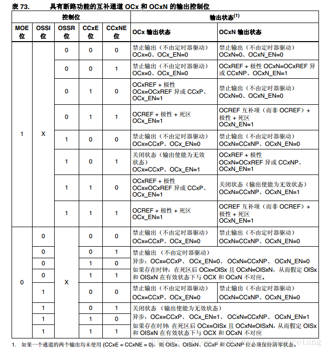
First, let's look at the OSSR bit. This bit is valid when MOE=1, that is, in the running mode. When it is configured to 0, when OC1REF is in an invalid state, the output is disabled, which is equivalent to clearing CC1E and CC1NE to 0. When OC1REF is in a valid state, and CC1E and CC1NE are both enabled, the output level is output according to the configuration of CC1NP and CC1P. When it is configured to 1, it has no effect on the output. Let's look at the OSSI bit. This is configured to take effect when MOE=0. Use the following table to understand it as a whole:
It should be noted that when OC1E and OC1NE are both set to the enabled state, the level of OC1 output is OC1REF + polarity, and the level of OC1N output is OC1REF's complementary phase + polarity. Having said so much about output control, STM32 is so complicated in order to be applied in complex occasions, such as the application of dead zone:
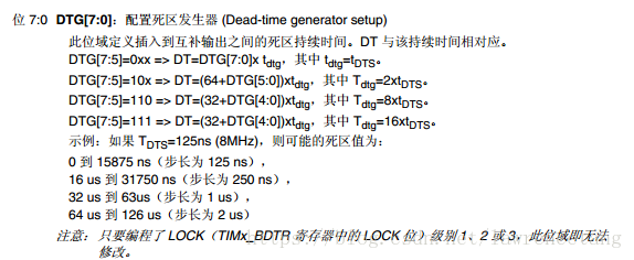
A typical dead time sequence diagram, with complementary outputs of OCX and OCXN plus a dead time. We have already discussed how to configure complementary outputs, but how to configure the dead time? The configuration is done through the DTG bit:
Look, tDTS is used again, and I am back to what I talked about at the beginning. Well, I wrote so much to summarize the knowledge I learned before. Although it is relatively simple and I just copy it, it is still beneficial to summarize it. I originally wanted to write it together with the HAL library, but as the saying goes, "Time flies like an arrow", let it go.
Previous article:STM32 timer (TIM) general timer
Next article:STM32 external interrupt and timer programming example
- Popular Resources
- Popular amplifiers
- Learn ARM development(16)
- Learn ARM development(17)
- Learn ARM development(18)
- Embedded system debugging simulation tool
- A small question that has been bothering me recently has finally been solved~~
- Learn ARM development (1)
- Learn ARM development (2)
- Learn ARM development (4)
- Learn ARM development (6)
 Professor at Beihang University, dedicated to promoting microcontrollers and embedded systems for over 20 years.
- LED chemical incompatibility test to see which chemicals LEDs can be used with
- Application of ARM9 hardware coprocessor on WinCE embedded motherboard
- What are the key points for selecting rotor flowmeter?
- LM317 high power charger circuit
- A brief analysis of Embest's application and development of embedded medical devices
- Single-phase RC protection circuit
- stm32 PVD programmable voltage monitor
- Introduction and measurement of edge trigger and level trigger of 51 single chip microcomputer
- Improved design of Linux system software shell protection technology
- What to do if the ABB robot protection device stops
- Analysis of the application of several common contact parts in high-voltage connectors of new energy vehicles
- Wiring harness durability test and contact voltage drop test method
- From probes to power supplies, Tektronix is leading the way in comprehensive innovation in power electronics testing
- From probes to power supplies, Tektronix is leading the way in comprehensive innovation in power electronics testing
- Sn-doped CuO nanostructure-based ethanol gas sensor for real-time drunk driving detection in vehicles
- Design considerations for automotive battery wiring harness
- Do you know all the various motors commonly used in automotive electronics?
- What are the functions of the Internet of Vehicles? What are the uses and benefits of the Internet of Vehicles?
- Power Inverter - A critical safety system for electric vehicles
- Analysis of the information security mechanism of AUTOSAR, the automotive embedded software framework
- APWM
- Industrial computer case
- EEWORLD University Hall----Live Replay: Datang NXP-DNS Battery Management Chip Solution
- 5G Network Slicing
- Static Electricity Protection Measures in Circuits
- Portable energy storage power supply-Nanxin Semiconductor enters the market with strength
- Summary of the characteristics of 5 wireless transmission protocols for the Internet of Things
- Can dual 12V power supplies be used in parallel?
- MSP-FET430UIF driver cannot be installed in Windows 7
- Use GD32 to make a music spectrum to practice















 RM4077AT/883B


 京公网安备 11010802033920号