1. Bus
system structure
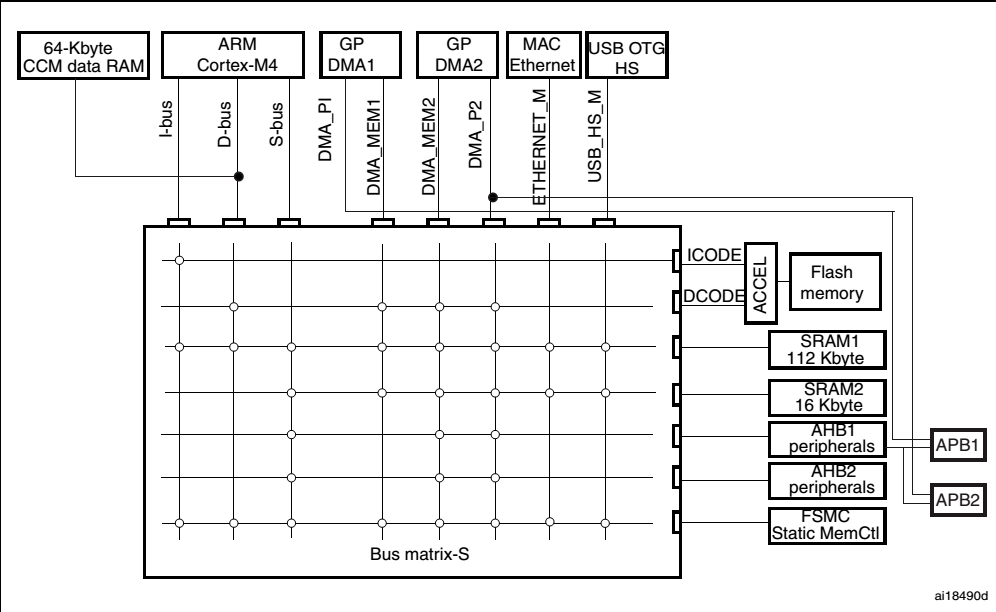
The system consists of a matrix of multiple interconnected 32-bit AHB buses
8 main buses
    – Cortex-M4 with FPU core I-bus, D-bus and S-bus
    – DMA1 memory bus
    – DMA2 memory bus
    – DMA2 peripheral bus
    – Ethernet DMA bus
    – USB OTG HS DMA bus123456
7 slave buses:
    – Internal Flash memory ICode bus
    – Internal Flash memory DCode bus
    – Main internal SRAM1 (112 KB)
    – Auxiliary internal SRAM2 (16 KB)
    – AHB1 peripherals including AHB to APB bridges and APB peripherals
    – AHB2 peripherals
    – FSMC1234567
The bus matrix also provides master-to-slave access, thus enabling concurrent access and efficient operation even when multiple high-speed peripherals are operating simultaneously. The 64Kbyte CCM (core coupled memory) data RAM is not part of the bus matrix and can only be accessed by the CPU.
Bus type
I-bus
This bus connects the instruction bus of the Cortex-M4 core with FPU to the BusMatrix. This bus is used by the core for instruction fetch operations. The control target of this bus is a piece of memory containing code (internal Flash memory/SRAM or external memories through the FSMC/FMC).
D-bus
This bus connects the data bus of the Cortex-M4 core with FPU to the 64Kbyte CCM data RAM and then to the BusMatrix. This bus is used by the core to download code and debug. The control target of this bus is a piece of memory containing code or data (internal Flash memory or external memories through the FSMC/FMC).
S-bus
This bus connects the system bus of the Cortex-M4 core with FPU to the BusMatrix. This bus is used to access data loaded into SRAM or peripherals. Instructions may also be obtained through this bus (not as efficient as ICode). The control targets of this bus are: internal SRAM1, SRAM2 and SRAM3, AHB1 peripherals (including APB peripherals), AHB2 peripherals and external memory through FSMC/FMC
BusMatrix
The BusMatrix manages access arbitration between bus masters. Arbitration uses a round-robin algorithm
Bus structure diagram:
2. Memory distribution
Programming space (code space), data space, registers and I/O ports are organized in the same linear 4Gb space. All data is stored in little-endian format.
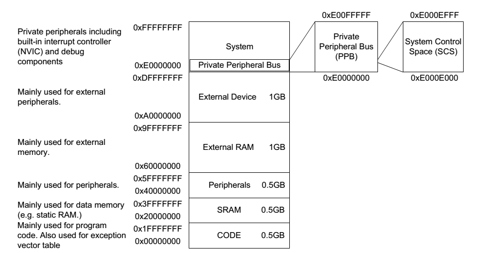
The addressable memory space is divided into 8 blocks, each containing 512MB
All space that is not allocated to on-chip memory or on-chip peripherals is called "reserved"
Embedded SRAM
The STM32F407ZG is configured with 4 Kbytes of backup SRAM and 192 Kbytes of system SRAM.
The embedded SRAM can be accessed in byte, half-word, or word mode, and can be accessed at the CPU speed without waiting. The embedded SRAM is divided into the following three blocks:
SRAM1 and SRAM2 are mapped to address 0x2000 0000 and can be accessed by all AHB buses.
SRAM3 (only available in STM32F42xxx and STM32F43xxx series) is mapped at address 0x2002 0000 and can be accessed by all AHB buses
CCM (core coupled memory) is mapped to address 0x1000 0000 and can only be accessed by the CPU via D-bus
Bit-band operation
In STM32, two bit-band operation domains and corresponding bit-band alias domains are provided.
| Bit-band operation field | Alias domain |
|---|---|
| The lower 1M bytes of SRAM: 0x2000 0000~0x200F FFFF | 0x2200 0000~0x23FF FFFC |
| The lower 1M bytes of the peripherals: 0x4000 0000~0x400F FFFF | 0x4200 0000~0x43FF FFFC |
Bit band operation formula:
bit_word_addr = bit_band_base + (byte_offset x 32) + (bit_number × 4)1
example:
0x22006008 = 0x22000000 + (0x300*32) + (2*4)/* Reading and writing 0x22006008 realizes reading and writing the second bit at 0x2000 0300 *//* Similarly, if you want to perform bit operations on the 0x40000000 address block, you need to replace 0x22000000 on the right side of the above formula with 0x42000000 */123
In the future, when we want to directly operate a certain bit of a register, we only need to find the alias address corresponding to this bit, and then read and write the alias address to achieve the reading and writing of this bit. If you want to achieve this operation, you only need to define a macro, such as the following:
#define REGISTER_BIT_BAND(ofs, bit_num) (0x22000000 + (ofs << 5) + (bit_num << 2))
#define WRITE_R_BIT_BAND(ofs, bit_num, stat) (*((volatile unsigned int *)REGISTER_BIT_BAND(ofs, bit_num)) = stat) // The above two macros can be used to operate on the register bit band domain 123
The M series 4GB memory layout given in the kernel programming manual
3. Startup Configuration
Startup method
| Boot mode selection pins | Boot mode | Aliasing | |
|---|---|---|---|
| BOOT1 | BOOT0 | ||
| x | 0 | Main Flash memory | Main Flash memory is selected as the boot space |
| 0 | 1 | System memory | System memory is selected as the boot space |
| 1 | 1 | Embedded SRAM | Embedded SRAM is selected as the boot space |
My board starts in the main flash memory. From the previous ARM compiler tool section, we know that the code starts running from 0x08000000. This is also specified by the scatter loading file and is also the actual address of the main flash on the board.
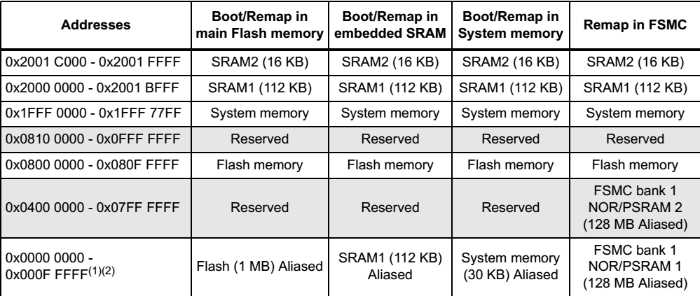
Physical address remapping
The following memory spaces can be remapped:
- Main Flash memory- System memory- Embedded SRAM1 (112 KB)- FSMC bank 1 (NOR/PSRAM 1 and 2)1234
The mapping table is
The memory block mapped to the address 0x00000000 can be determined by the lower two bits of the SYSCFG controller (SYSCFG_MEMRMP) register, as shown in the following table
| bit1 | bit0 | memory selected |
|---|---|---|
| 0 | 0 | Main Flash memory mapped at 0x0000 0000 |
| 0 | 1 | System Flash memory mapped at 0x0000 0000 |
| 1 | 0 | FSMC Bank1 (NOR/PSRAM 1 and 2) mapped at 0x0000 0000 |
| 1 | 1 | Embedded SRAM (SRAM1) mapped at 0x0000 0000 from the table |
It can be seen that when starting from the main flash, the flash memory will be remapped to address 0, with a size of 1MB, but my board still runs the code from address 0x08000000. Now from the data in the table, it can be seen that it is also possible to run from address 0. It may be to adapt to different startup methods, so the system code is run from address 0x08000000. If you want to run the code in the flash memory from other places, you only need to add a jump statement at the beginning of the code segment that is remapped to address 0 in that way, and jump directly to address 0x08000000 to run the code.
4. Embedded flash memory
Interface features:
Flash memory read operation
Flash memory program/erase operations
Read/write protection
Instruction Prefetch
I-Code has 64 128-bit wide fast access lines
I-Code has eight 128-bit wide fast access lines
Flash memory features:
1M byte capacity
128-bit read data width
Support Byte, half-word, word and double word writing
Support sector and block erase
Support memory organization
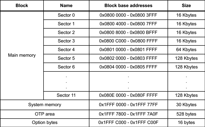
– The main memory is divided into 4 sectors of 16 Kbytes, 1 sector of 64 Kbytes, and 7 sectors of 128 Kbytes
– Different boot devices correspond to corresponding system memory
– 512 OTP (One Time Programming) bytes
- Optional read and write protection
The flash memory can be organized as follows:
Low Power Mode
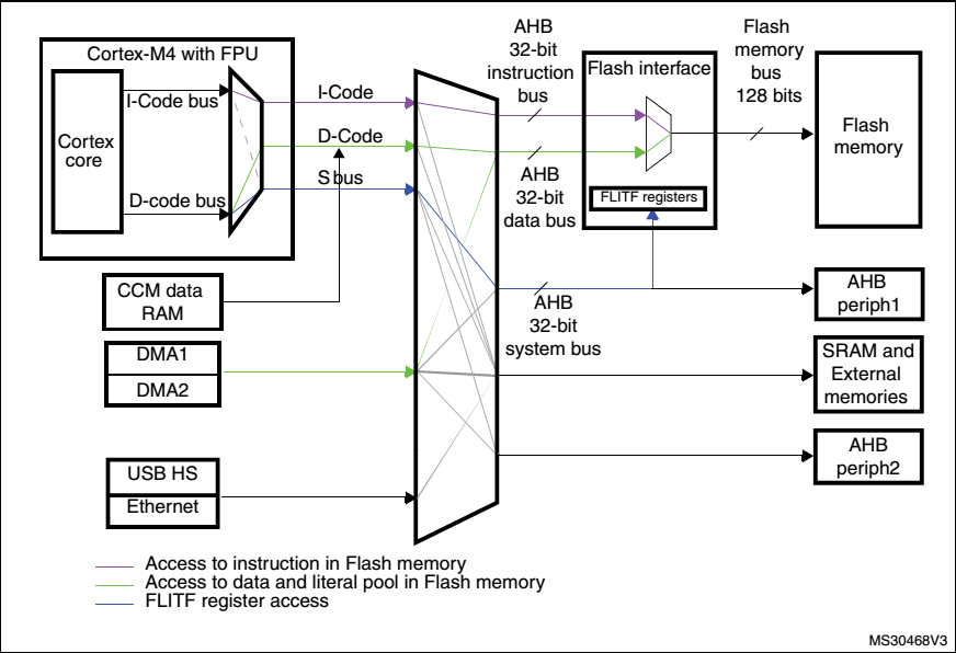
Memory distribution diagram
Additional content of the clock section:
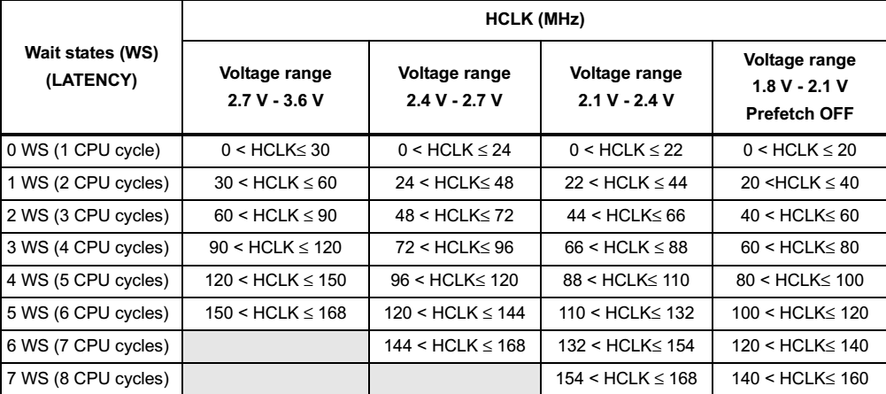
VOS is set in bit 15 of the PWR_CR register.
When VOS = '0', the maximum fHCLK is 144 MHz.
When VOS = '1', the maximum fHCLK is 168 MHz.
Waiting cycle
The waiting cycle refers to the waiting time for the CPU to access the Flash. The cycle for the CPU to access the Flash is the waiting cycle plus 1. This is related to the hardware performance of the Flash.
Previous article:Differences between STM32F4 and STM32F1
Next article:STM32 Core Coupled Memory (CCM)
- Popular Resources
- Popular amplifiers
- Learn ARM development(16)
- Learn ARM development(17)
- Learn ARM development(18)
- Embedded system debugging simulation tool
- A small question that has been bothering me recently has finally been solved~~
- Learn ARM development (1)
- Learn ARM development (2)
- Learn ARM development (4)
- Learn ARM development (6)
 Professor at Beihang University, dedicated to promoting microcontrollers and embedded systems for over 20 years.
- LED chemical incompatibility test to see which chemicals LEDs can be used with
- Application of ARM9 hardware coprocessor on WinCE embedded motherboard
- What are the key points for selecting rotor flowmeter?
- LM317 high power charger circuit
- A brief analysis of Embest's application and development of embedded medical devices
- Single-phase RC protection circuit
- stm32 PVD programmable voltage monitor
- Introduction and measurement of edge trigger and level trigger of 51 single chip microcomputer
- Improved design of Linux system software shell protection technology
- What to do if the ABB robot protection device stops
- Analysis of the application of several common contact parts in high-voltage connectors of new energy vehicles
- Wiring harness durability test and contact voltage drop test method
- From probes to power supplies, Tektronix is leading the way in comprehensive innovation in power electronics testing
- From probes to power supplies, Tektronix is leading the way in comprehensive innovation in power electronics testing
- Sn-doped CuO nanostructure-based ethanol gas sensor for real-time drunk driving detection in vehicles
- Design considerations for automotive battery wiring harness
- Do you know all the various motors commonly used in automotive electronics?
- What are the functions of the Internet of Vehicles? What are the uses and benefits of the Internet of Vehicles?
- Power Inverter - A critical safety system for electric vehicles
- Analysis of the information security mechanism of AUTOSAR, the automotive embedded software framework
- What knowledge do you need to do LED lighting?
- Various types of timers and clocks for MSP430
- How to use high-speed ADC and DAC with FPGA.pdf
- Lisp Badge (uList Badge)
- UART1 idle interrupt exception occurs when STM32F407VE replaces STM32F429VI
- C++ inheritance important understanding
- [SC8905 EVM Evaluation] + Use of the setting tool SC9805tool
- [IDE] Does IAR have a function module similar to Keil's RTE?
- FPGA Learning Experience
- The best NUCLEO-G474RE has arrived

 TC913BCOATR


 京公网安备 11010802033920号