1. Scheme demonstration and selection
1.1 Solution selection
1.1.1 Signal generation module
Solution 1: Use analog discrete components or a single-chip voltage-controlled function generator. It can generate sine waves, square waves, and triangle waves at the same time, but due to the large dispersion of the components, the generated frequency stability is poor, the accuracy is low, the waveform is poor, and arbitrary waveform output cannot be achieved.
Solution 2: Use traditional direct frequency synthesizer. This method can achieve fast frequency conversion, low phase noise and the highest operating frequency of all methods. However, due to the use of a large number of frequency multiplication, frequency division, mixing and filtering links, the structure of direct frequency synthesis is complicated, and it cannot achieve arbitrary waveform output.
Solution 3: Use phase-locked frequency synthesizer. Phase-locked frequency synthesis is a technology that generates a large number of discrete frequencies with the same stability and accuracy through addition, subtraction, multiplication and division operations on a standard frequency with high stability and accuracy. It solves the contradiction between stable and accurate frequency and variable frequency in a large range to a certain extent. However, since the phase-locked loop itself is an inert link and the locking time is long, the frequency conversion time is long and the frequency is limited. The more important weakness is that the function of arbitrary waveform cannot be realized.
Solution 4: Use direct digital frequency synthesizer (DDFS). DDFS technology is based on the Nyquist time-domain sampling theorem and performs frequency synthesis in the time domain. It can quickly change the frequency and realize arbitrary waveform functions by changing the waveform data. DDFS has a relatively high bandwidth, continuous output phase, and the frequency, phase and amplitude can be program-controlled. Make full use of the internal resources of FPGA and set all logic circuits inside it to realize DDS synthesis. Theoretically, it can reach MHz. The frequency band requirement of 100 kHz is easy to achieve, and most of the hardware is omitted. Only D/A conversion output is required to avoid the influence of the division of hardware circuits.
In order to reduce the hardware burden as much as possible and make full use of digital resources, on the basis of meeting application requirements, option 4 is selected to implement frequency synthesis inside the FPGA.
1.1.2 Tested Network
Solution 1: Directly use the RC double-T network. The center frequency can be changed by changing the parameters of the capacitor and resistor, but its transfer function form is fixed, the bandwidth is about 4 times the center frequency, the Q value is fixed at 0.25, and the notch effect is poor.
Solution 2: Using an improved double-T network, the network output is fed back to the network through an emitter follower, which can limit the bandwidth and easily meet application requirements. Therefore, Solution 2 is selected.
1.2 System overall implementation block diagram
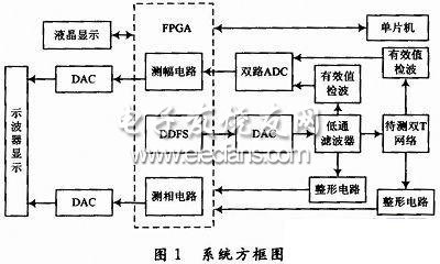
The system block diagram is shown in Figure 1.
2 Theoretical analysis and calculation
2.1 DDS Principle Analysis
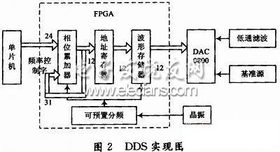
DDS is a method of generating signal waveforms using digital technology. Its main components are: phase accumulator, waveform memory, D/A converter and low-pass filter. The basic working principle is: under the control of the reference clock signal, the phase code is output through the phase accumulator controlled by the frequency control word K, and the waveform quantization sampling data value stored in the waveform memory is read out according to a certain rule, and the waveform is output after D/A conversion and low-pass filtering. The internal implementation block diagram of FPGA is shown in Figure 2.
Before implementing frequency synthesis through DDS technology, it is necessary to determine the main performance parameters of DDS:
Assume that the reference frequency source frequency is fclk, a phase accumulator with a counting capacity of 2N is used (N is the number of bits of the phase accumulator), and the frequency control word is M. The frequency of the DDS system output signal is fout=fclk/2N×M, and the frequency resolution is △f=fclk/2N. If the crystal frequency is selected as 40 MHz, the frequency control word is 24 bits, and the number of bits of the phase accumulator is 31 bits, the logic block diagram of the DDS module is shown in Figure 3. The theoretical output frequency range is 0.02 Hz to 312 kHz, and the step is about 0.02 Hz (40 MHz/231).
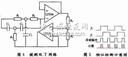
2.2 Dual T Network
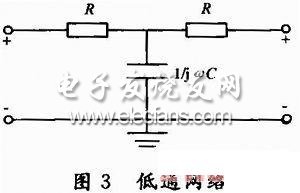
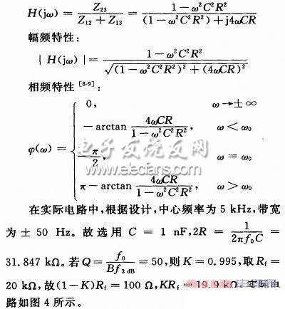
The double-T network can be considered as a T-type low-pass network and a T-type high-pass network. The low-pass network is shown in Figure 3. The resistance and capacitance are all converted into impedance representation. The transfer function H(jω) is:
2.3 Phase Measurement
This module adopts a multi-cycle synchronous counting method. The input signal cycle is filled with pulse counting. The specific method is as follows: a D flip-flop is used to generate a synchronous gate signal with a width of an integer number of the measured signal cycles. The synchronous gate signal and the clock pulse signal are ANDed and sent to counter 1 for counting. The count value is N1; the synchronous gate signal, the phase detection pulse and the clock pulse are ANDed and sent to counter 2 for counting. The count value is N2, and the phase difference is φx=(N2/N1)×180. This can greatly reduce the quantization error and improve the measurement accuracy, as shown in Figure 5.
Implementing gate settings, pulse calculations, counting, and other issues within the FPGA can increase system flexibility and measurement accuracy and reduce hardware workload.
3 Design of main functional circuits
3.1 DDS signal generation module
The AD9851 module processes the frequency control word sent by the microcontroller, outputs the address value to the ROM 1P module, the ROM 1P module stores the sine wave table, and outputs the amplitude value to the DA. The specific implementation in the FPGA is shown in Figure 6.

3.2 True RMS Measurement Circuit
A typical true RMS current conversion chip AD637 is used, which has few peripheral components and wide bandwidth. For a signal with an RMS value of 200mV, the -3 dB bandwidth is 600 kHz; for a signal with an RMS value of 1 V, the -3 dB bandwidth is 8 MHz, followed by a 12-bit high-speed, low-power serial analog/digital conversion chip ADS7818. In order to simplify the circuit and maintain the symmetry of the circuit parameters, only one ADS7818 is used, which is controlled by a single-chip microcomputer through an electromagnetic relay and periodically switches between the two signals for amplitude measurement.
3.3 Amplification, shaping and phase measurement module
Since the signal amplitude attenuated greatly after passing through the double-T network, and the transmission time of the signal through the zero-crossing comparator is

, where G0 is the DC gain of the zero-crossing detector; fP1 is the first response pole; f is the signal frequency; and VP is the signal amplitude. It can be seen from the formula that the amplitude is inversely proportional to the phase shift, so a stage of amplification is required before passing through the comparator. The automatic gain control circuit composed of the variable gain amplifier chip AD603 is used. When the peak-to-peak value of the input signal is between 400 mV and 7 V and the frequency is below 6 MHz, the output signal is stable and flat. In the actual circuit of this application, the input signal with an effective value ranging from 200 mV to 3.5 V and a frequency ranging from 30 Hz to 3 MHz is amplified to 1.72 V without distortion. Since the output voltage of DDS is 1.72 V, only the signal after passing through the network needs to be amplified. In addition, since the front stage is the emitter-follower in the double-T network, impedance matching is not required. The AGC (automatic gain control) circuit is shown in Figure 7.
The output signal is shaped by the hysteresis comparator near the zero point composed of LM311 and then sent to the FPGA for phase measurement. After amplification and shaping, the two signals first pass through the first-level polarity discrimination circuit, and the output level of the D flip-flop is read to determine whether the phase of the signal output from the dual-T network is ahead or behind the original signal phase. When the VOUT output is high, it is ahead, otherwise it is behind. At the same time, the two signals are sent to the XOR gate to obtain the pulse signal, measure the width of the pulse signal, and then calculate the phase difference. When the pulse width is very small, in order to meet the design requirements, the frequency of the standard pulse is required to be very high. A 40 MHz crystal oscillator was used in the design, so the expression of the phase difference is degrees.
3.4 Oscilloscope display module
The amplitude-frequency-phase-frequency information is added to the y-axis, and the frequency sawtooth wave is added to the x-axis. The D/A conversion uses the 12-bit serial port voltage output type programmable bias digital/analog conversion chip TLV5638.
4 Test Data and Analysis
4.1 Test Data Results
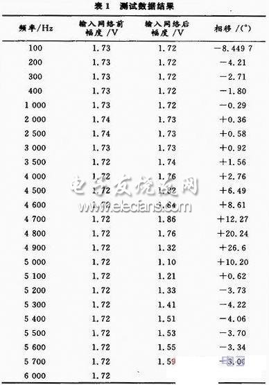
The test data results are shown in Table 1.
4.2 Data Analysis
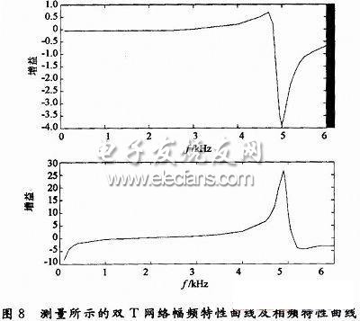
After measurement, the amplitude-frequency and phase-frequency characteristic curves of the double-T network are shown in Figure 8. In the amplitude-frequency characteristic curve, the horizontal axis represents frequency, one grid represents 1 kHz; the vertical axis represents gain, one grid represents 0.5 times. In the phase-frequency characteristic curve, the horizontal axis represents frequency, one grid represents 1 kHz; the vertical axis represents phase, one grid represents 5°.
4.3 Error Analysis
4.3.1 Phase measurement error analysis
(1) Counting error. The counter always has an error of ±1. This error exists in the scheme itself and cannot be eliminated. Although the improved counting scheme cannot eliminate the error, it can reduce the impact of the error.
(2) Errors introduced by pre-processing. Before using the counting method to measure phase, the two input signals need to be limited, amplified, and level-converted. Since it is difficult to ensure that the linearity of the circuits processing the two signals is completely consistent, errors will be introduced. In addition, during level conversion, the comparator will affect the instability of the rising or falling edge of the converted square wave, affecting the counting result.
(3) After the two signals are different or equal, the phase difference is measured by counting method. The standard clock signal is generated by a crystal oscillator. A 40 MHz crystal oscillator is used. The frequency stability of the crystal oscillator will also affect the measurement results.
(4) The phase difference measurement accuracy can be improved. If the phase difference accuracy is to reach 0.1°, the sine wave table data should store at least 360×10 points, but only 1024 points are stored here.
(5) The frequency sweeping DDS part can also improve the frequency sweeping accuracy. The frequency sweeping accuracy can be improved by increasing the FPGA internal clock frequency. The frequency sweeping reference clock uses 10 MHz. Because the D/A conversion part uses DAC0800 with a conversion speed of 100 ns, the reference clock frequency can be further increased, and the DAC0800 conversion speed can be fully achieved.
4.3.2 Amplitude measurement error analysis
Amplitude measurement uses true RMS detection. The AD637 chip itself has a fixed deviation when detecting the RMS value, but the deviations produced for the previous and subsequent signals are consistent, and the measurement results can be calibrated through software.
5 Summary, Analysis and Conclusion
Experiments show that the frequency sweep range of the DDS signal generation part is 100 Hz to 100 kHz, with a frequency step of 10 Hz. Users can select fixed-point measurement or specific frequency band sweep measurement by pressing buttons, and can display the preset frequency, signal amplitude before and after the network, phase difference and polarity through the LCD, and can also display the amplitude-frequency characteristic and phase-frequency characteristic curves on the oscilloscope. In addition, fixed-point measurement and specific frequency band measurement can be easily realized, which can help to understand the frequency characteristics well, and it has good scalability. The designed product is small in size and easy to carry, suitable for applications in teaching and other fields.
Previous article:Design of Ultrasonic Distance Meter with Temperature Compensation Based on Single Chip Microcomputer
Next article:Design and implementation of an electric bicycle controller tester
Recommended ReadingLatest update time:2024-11-17 01:26


- Popular Resources
- Popular amplifiers
-
 Analysis and Implementation of MAC Protocol for Wireless Sensor Networks (by Yang Zhijun, Xie Xianjie, and Ding Hongwei)
 -
 MATLAB and FPGA implementation of wireless communication
 -
 西门子S7-12001500 PLC SCL语言编程从入门到精通 (北岛李工)
 -
 Siemens Motion Control Technology and Engineering Applications (Tongxue, edited by Wu Xiaojun)
 Professor at Beihang University, dedicated to promoting microcontrollers and embedded systems for over 20 years.
- Innolux's intelligent steer-by-wire solution makes cars smarter and safer
- 8051 MCU - Parity Check
- How to efficiently balance the sensitivity of tactile sensing interfaces
- What should I do if the servo motor shakes? What causes the servo motor to shake quickly?
- 【Brushless Motor】Analysis of three-phase BLDC motor and sharing of two popular development boards
- Midea Industrial Technology's subsidiaries Clou Electronics and Hekang New Energy jointly appeared at the Munich Battery Energy Storage Exhibition and Solar Energy Exhibition
- Guoxin Sichen | Application of ferroelectric memory PB85RS2MC in power battery management, with a capacity of 2M
- Analysis of common faults of frequency converter
- In a head-on competition with Qualcomm, what kind of cockpit products has Intel come up with?
- Dalian Rongke's all-vanadium liquid flow battery energy storage equipment industrialization project has entered the sprint stage before production
- Allegro MicroSystems Introduces Advanced Magnetic and Inductive Position Sensing Solutions at Electronica 2024
- Car key in the left hand, liveness detection radar in the right hand, UWB is imperative for cars!
- After a decade of rapid development, domestic CIS has entered the market
- Aegis Dagger Battery + Thor EM-i Super Hybrid, Geely New Energy has thrown out two "king bombs"
- A brief discussion on functional safety - fault, error, and failure
- In the smart car 2.0 cycle, these core industry chains are facing major opportunities!
- Rambus Launches Industry's First HBM 4 Controller IP: What Are the Technical Details Behind It?
- The United States and Japan are developing new batteries. CATL faces challenges? How should China's new energy battery industry respond?
- Murata launches high-precision 6-axis inertial sensor for automobiles
- Ford patents pre-charge alarm to help save costs and respond to emergencies
- [EEWorld invites you to play disassembly] ROMOSS power bank 30000 mAh 22.5W
- Q&A Session: The most important components of the analog world - signal chain and power supply
- Permanent Magnet Stepper Motor Identification Experience and Techniques
- GPIO block diagram of C6000 series DSP
- EEWORLD University Hall----Live Replay: TI desktop DLP 3D printing, 3D scanning and industrial display applications based on DLP? Pico? technology
- We are looking for candidates who are proficient in zigbee!
- 【MM32 eMiniBoard Review】2a. Found that the virtual serial port may have problems, and the serial port routines cannot receive
- Help! Does anyone know what sensor this is?
- ADC12 single channel multiple conversion routine (MSP430F5529)
- Motor startup interferes with the microcontroller problem

 Analysis and Implementation of MAC Protocol for Wireless Sensor Networks (by Yang Zhijun, Xie Xianjie, and Ding Hongwei)


 京公网安备 11010802033920号