Over the past two years, Google has been working to make silicon design more open source to promote the development of more chip manufacturing projects. Through its initial collaboration with SkyWater, the tech giant hopes to help project participants reduce the cost burden of open source chips. In late July, Google announced that its open source silicon design toolkit with SkyWater was moving to 90nm. Now, the company has reached a 180nm process collaboration with GlobalFoundries.

(Source: Google Open Source Blog)
In a Google open source blog post published on Wednesday, the company's open source team announced that GlobalFoundries has become the latest member to join its "Open Chip Initiative" and provide access to 180nm chip manufacturing technology.
Google and GlobalFoundries today jointly released the open source Process Design Kit (PDK) for GlobalFoundries' 180nm/180MCU technology platform.
The PDF documentation is available under the Apache 2.0 license, and Google will have a free Efabless silicon implementation project to create an open source design (similar to the SkyWater project).

Google/gf180mcu-pdk (GitHub)
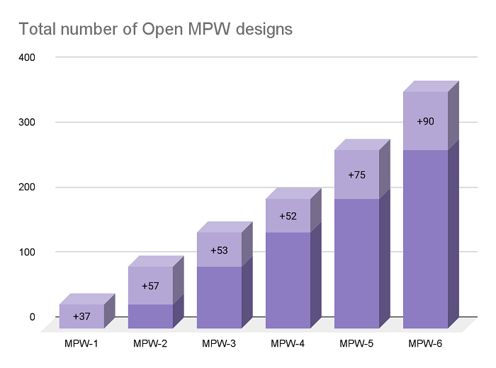
Google has actively promoted six times in the past two years, providing assistance for more than 350 unique silicon designs, and about 240 of them have been built for free.
Now, with access to SkyWater 90nm and GlobalFoundries 180nm processes, Google's vision of open source silicon design will be more widely used.

Although from the perspective of the "advancedness" of the process, the number 180nm is not very exciting, after all, current high-end processors have generally embraced 7nm (or even below 5nm).
However, Phoronix pointed out that the mature 180nm process is still quite applicable in areas such as the Internet of Things, automotive, and MCU/PMIC.
GlobalFoundries expects that its 180nm process will achieve growth of more than 22 million wafers by 2026 (currently annual output is only 16 million+).
Previous article:SMART Modular launches its first CXL memory module
Next article:Intel is reportedly close to reaching a $5 billion factory construction agreement with the Italian government
- Popular Resources
- Popular amplifiers
- ASML provides update on market opportunities at 2024 Investor Day
- It is reported that memory manufacturers are considering using flux-free bonding for HBM4 to further reduce the gap between layers
- Intel China officially releases 2023-2024 Corporate Social Responsibility Report
- Mouser Electronics and Analog Devices Launch New E-Book
- AMD launches second-generation Versal Premium series: FPGA industry's first to support CXL 3.1 and PCIe Gen 6
- SEMI: Global silicon wafer shipment area increased by 6.8% year-on-year and 5.9% month-on-month in 2024Q3
- TSMC's 5nm and 3nm supply reaches "100% utilization" showing its dominance in the market
- LG Display successfully develops world's first stretchable display that can be expanded by 50%
- Infineon's revenue and profit both increased in the fourth quarter of fiscal year 2024; market weakness in fiscal year 2025 lowered expectations
- LED chemical incompatibility test to see which chemicals LEDs can be used with
- Application of ARM9 hardware coprocessor on WinCE embedded motherboard
- What are the key points for selecting rotor flowmeter?
- LM317 high power charger circuit
- A brief analysis of Embest's application and development of embedded medical devices
- Single-phase RC protection circuit
- stm32 PVD programmable voltage monitor
- Introduction and measurement of edge trigger and level trigger of 51 single chip microcomputer
- Improved design of Linux system software shell protection technology
- What to do if the ABB robot protection device stops
- CGD and Qorvo to jointly revolutionize motor control solutions
- CGD and Qorvo to jointly revolutionize motor control solutions
- Keysight Technologies FieldFox handheld analyzer with VDI spread spectrum module to achieve millimeter wave analysis function
- Infineon's PASCO2V15 XENSIV PAS CO2 5V Sensor Now Available at Mouser for Accurate CO2 Level Measurement
- Advanced gameplay, Harting takes your PCB board connection to a new level!
- Advanced gameplay, Harting takes your PCB board connection to a new level!
- A new chapter in Great Wall Motors R&D: solid-state battery technology leads the future
- Naxin Micro provides full-scenario GaN driver IC solutions
- Interpreting Huawei’s new solid-state battery patent, will it challenge CATL in 2030?
- Are pure electric/plug-in hybrid vehicles going crazy? A Chinese company has launched the world's first -40℃ dischargeable hybrid battery that is not afraid of cold
- About the version of MicroPython?
- 2019 National Undergraduate Electronic Design Competition Summary and Award Ceremony Notice
- Disease data information is uploaded to the cloud in a timely manner NRF9160
- Measuring magnet position using the LSM303AGR magnetometer
- [Silicon Labs BG22-EK4108A Bluetooth Development Evaluation] 2. Development Environment Construction
- It’s not fun anymore. The delivery time of 4G modules is about 4-6 weeks.
- ARM or x86? Who will stand out in the future industrial SBC digital industry?
- ST MEMS Device Resource Library-Development Platform Application Guide
- A new low-cost miniaturized GPS antenna
- This factory will run on 100% renewable energy!

 6884-700


 京公网安备 11010802033920号