The VLSI Symposium will be held June 12-17 at the Hilton Hawaiian Village in Honolulu. Samsung will present 18 papers at the conference.
In the DRAM memory category, Samsung will release "A 16 GB 1024 GB/s HBM3 DRAM with On-Die Error Control".
Samsung’s third-generation 10nm DRAM (1z) features higher system reliability, availability and serviceability (RAS) performance and is targeted at automotive, industrial and data center applications.
To do this, they used a new on-chip error correction (ECC) scheme that can correct 16-bit word errors and 2 individual bit errors simultaneously, and incorporated it into a new version of "High Bandwidth Memory-3" (HBM3) DRAM.
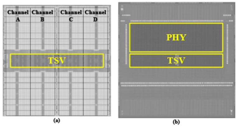
Micrograph of Samsung's HBM3 chip: (a) core and (b) buffer
Local corrections are made on each individual DRAM die, rather than accessing the rest of the stack, which reduces latency and increases the pin data rate to 8.0Gb/s/pin from the previous generation’s 5Gb/s/pin, bringing the total memory bandwidth to 1024GB/s per memory die, as demonstrated in a 16GB DRAM module.
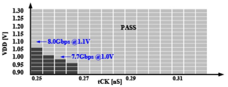
Measured clock frequency of Samsung's HBM3 chip
Samsung’s 3nm gate-all-around FET (GAA FET) technology was demonstrated in “A 3nm GAAFET Analog Assisted Digital LDO with High Current Density for Dynamic Voltage Scaling Mobile Applications.”
Discussed here is an analog-assisted digital LDO that provides high current density power delivery with active power supply noise cancellation and fast transient load detection for the CPU core.
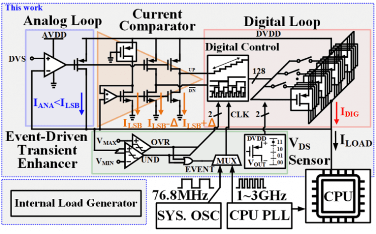
Samsung's hybrid LDO architecture for mobile SoC applications
This hybrid LDO design achieves precise regulation over the load range of <1 mA to 1.4 A, with only 38mV supply drop in 1ns to a 1A dynamic load.

Load curves of conventional and hybrid GAAFET LDOs
In addition, there is a paper on "A 0.6μm Small Pixel for High Resolution CMOS Image Sensor with Full Well Capacity of 10,000e- by Dual Vertical Transfer Gate Technology".
Samsung has developed a 200Mp image sensor prototype using 0.6μm pixels with a full charge well capacity (FWC) of 10,000e using dual vertical transfer gate (D-VTG) technology. Compared with a single vertical transfer gate, the FWC of D-VTG is increased by 60%, and the transfer performance is also improved due to the improved controllability of the transfer gate voltage.
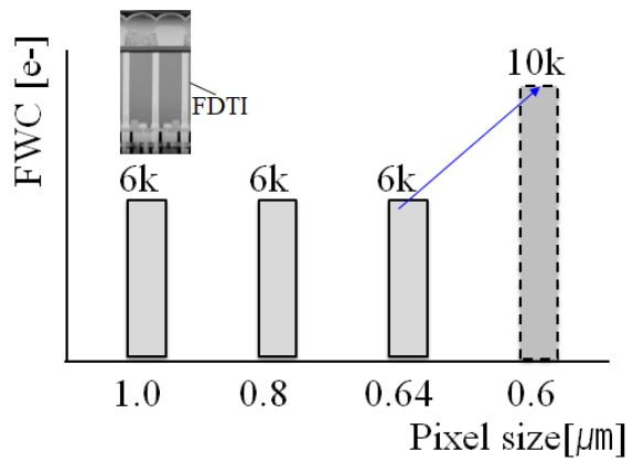
Samsung's full charge well capacity based on pixel size
Photoelectron transport is optimized by adjusting the gap, depth, and taper slope of the VTG, as shown in the figure below.
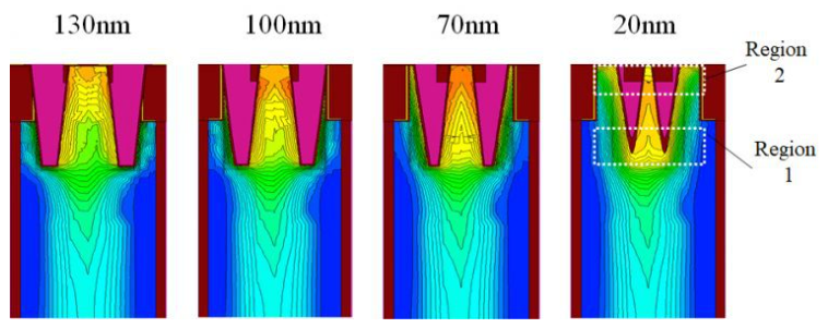
Relationship between the potential curve of the transfer gate and the spacing
In addition, other included papers include:
C10-1 A 12-bit 8GS/s RF Sampling DAC with Code-Dependent Nonlinearity Compensation and Intersegmental Current-Mismatch Calibration in 5-nm FinFET
C10-3 A 0.56mW 63.6dB SNDR 250MS/s SAR ADC in 8-nm FinFET
C11-5 Fully Integrated 2×2 MIMO Real Simultaneous Dual Band WiFi CMOS Power Amplifiers With a Single Inductor Multiple Output Supply Modulation Technique
C14-2 High Efficiency 29-/38-GHz Hybrid Transceiver Front-Ends Utilizing Si CMOS and GaAs HEMT for 5G NR Millimeter-Wave Mobile Applications
C15-2 A 32 Mb Embedded Flash Memory based on 28 nm with the best Cell Efficiency and Robust Design achievement featuring 13.48 Mb/mm2 at 0.85 V
C17-1 A 40-Gb/s/pin Low-Voltage POD Single-Ended PAM-4 Transceiver with Timing Calibrated Resetless Slicer and Bidirectional T-Coil for GDDR7 Application
C16-3 An Automotive ASIL-D Safety Mechanism in ADC and DAC for Communication Application
C18-5 Palm-sized LiDAR module with III/V-on-Si optical phased array
C19-3 A 12-bit 10GS/s 16-Channel Time-Interleaved ADC with a Digital Processing Timing-Skew Background Calibration in 5nm FinFET
C22-4 A 0.7 mm2 Power Management Unit for Implantable Electroceutical Device with a
91.4 % Peak Efficiency Buck-based Hybrid Step-up and -down MISIMO Converter
C24-4 4-nm Voltage Auto-Tracking SRAM Pulse Generator with Fully RC Optimized Row Auto-Tracking Write Assist Circuits
TFS1-2 Prospective Innovation of DRAM, Flash, and Logic Technologies for Digital Transformation (DX) Era
T8-5 Advanced novel optical stack technologies for high SNR in CMOS Image Sensor
T10-1 Standard Cell Design Optimization with Advanced MOL Technology in 3-nm GAA Process
T10-4 Comprehensive Feasibility Study of Single FIN Transistors for Scaling Both Switching Energy and Device Footprint
Previous article:Renesas Electronics invests in Kofu plant, 300mm power semiconductor production line resumes
Next article:STMicroelectronics and MACOM Successfully Pilot-Prototype GaN-on-Silicon
- Popular Resources
- Popular amplifiers
- The US asked TSMC to restrict the export of high-end chips, and the Ministry of Commerce responded
- ASML predicts that its revenue in 2030 will exceed 457 billion yuan! Gross profit margin 56-60%
- ASML provides update on market opportunities at 2024 Investor Day
- It is reported that memory manufacturers are considering using flux-free bonding for HBM4 to further reduce the gap between layers
- Intel China officially releases 2023-2024 Corporate Social Responsibility Report
- Mouser Electronics and Analog Devices Launch New E-Book
- AMD launches second-generation Versal Premium series: FPGA industry's first to support CXL 3.1 and PCIe Gen 6
- SEMI: Global silicon wafer shipment area increased by 6.8% year-on-year and 5.9% month-on-month in 2024Q3
- TSMC's 5nm and 3nm supply reaches "100% utilization" showing its dominance in the market
- LED chemical incompatibility test to see which chemicals LEDs can be used with
- Application of ARM9 hardware coprocessor on WinCE embedded motherboard
- What are the key points for selecting rotor flowmeter?
- LM317 high power charger circuit
- A brief analysis of Embest's application and development of embedded medical devices
- Single-phase RC protection circuit
- stm32 PVD programmable voltage monitor
- Introduction and measurement of edge trigger and level trigger of 51 single chip microcomputer
- Improved design of Linux system software shell protection technology
- What to do if the ABB robot protection device stops
- Apple faces class action lawsuit from 40 million UK iCloud users, faces $27.6 billion in claims
- Apple faces class action lawsuit from 40 million UK iCloud users, faces $27.6 billion in claims
- The US asked TSMC to restrict the export of high-end chips, and the Ministry of Commerce responded
- The US asked TSMC to restrict the export of high-end chips, and the Ministry of Commerce responded
- ASML predicts that its revenue in 2030 will exceed 457 billion yuan! Gross profit margin 56-60%
- Detailed explanation of intelligent car body perception system
- How to solve the problem that the servo drive is not enabled
- Why does the servo drive not power on?
- What point should I connect to when the servo is turned on?
- How to turn on the internal enable of Panasonic servo drive?
- Design of Intelligent Motor Protector Based on DSP
- Happy Teacher's Day! Let's talk about the teacher you remember most when you were in school!
- Definition of waveform overshoot on sampling resistor in constant current source application
- How to generate such waveform using Verilog?
- 【TI millimeter wave radar evaluation】_2_AWR1843BOOST usage
- Environmental Monitoring System
- Are only foreign companies exempt from overtime work?
- 06 Make GD32L233C expansion board
- The names, wavelengths, characteristics and application fields of each band in the electromagnetic spectrum
- [TI Course] How is the anti-interference ability of TI millimeter-wave radar?

 UA748MJG/883B


 京公网安备 11010802033920号