At TSMC's annual technology seminar, the characteristics of the future 3nm process node were introduced in detail, and a roadmap was planned for subsequent 5nm products, including the N5P and N4 process nodes.
Starting with TSMC's upcoming N5 process node, which represents the second generation of deep ultraviolet (DUV) and extreme ultraviolet (EUV) nodes after the rarely used N7+ node (used by the Kirin 990 SoC, for example). TSMC has already started volume production for a few months, and Apple's next-generation SoCs may be the first candidates for this node.
TSMC detailed that N5's current defect density is one-quarter better than N7, and the new node has a higher yield in mass production than its predecessor major nodes N7 and N10, and defect density is expected to continue to improve, exceeding the historical trend of the past two generations.
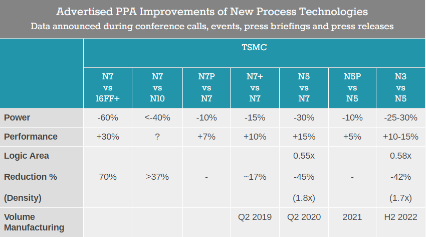
The foundry is also preparing a new N5P node, based on the current N5 process, that promises a 5% speed increase and 10% reduction in power consumption.
In addition to N5P, TSMC is also introducing the N4 node, which represents a further evolution of the N5 process, with more EUV layers to reduce masks, with minimal migration work required for chip designers. We will see N4 risk production start in Q4 2021, with volume production later in 2022.
The biggest news today is that TSMC disclosed their next-generation N5 process node family, the 3nm process N3. They started defining this node last year and are currently progressing smoothly.
Contrary to Samsung's 3nm process node's use of the GAA (Gate all around) transistor structure, TSMC will stick with FinFET transistors and rely on "innovative features" to achieve the full-node expansion promised by N3.
PPA improvement with new process technology

Compared to the N5 node, N3 promises to improve performance by 10-15% at the same power level, or reduce power by 25-30% at the same transistor speed. In addition, TSMC promises a 1.7x increase in logic area density. Of course, this shrinkage does not directly target all structures, the density of SRAM is only improved by 20%, and the analog structure will improve even less.
Modern chip designs are very SRAM-heavy, with a typical SRAM/logic split of 70/30, so at the chip level, the expected shrink is only 26% or less.
N3 is scheduled to enter risk production in 2021 and volume production in the second half of 2022. The process characteristics disclosed by TSMC on N3 will not differ much from the power and performance disclosed by Samsung on 3GAE, but will lead more in density.
Previous article:Under heavy pressure, China's IC imports and exports achieved double-digit growth in the first half of 2020!
Next article:Qualcomm's anti-competitive strategy has caused dissatisfaction among many companies
Recommended ReadingLatest update time:2024-11-15 15:06


- Popular Resources
- Popular amplifiers
- Vietnam's chip packaging and testing business is growing, and supply-side fragmentation is splitting the market
- The US asked TSMC to restrict the export of high-end chips, and the Ministry of Commerce responded
- ASML predicts that its revenue in 2030 will exceed 457 billion yuan! Gross profit margin 56-60%
- ASML provides update on market opportunities at 2024 Investor Day
- It is reported that memory manufacturers are considering using flux-free bonding for HBM4 to further reduce the gap between layers
- Intel China officially releases 2023-2024 Corporate Social Responsibility Report
- Mouser Electronics and Analog Devices Launch New E-Book
- AMD launches second-generation Versal Premium series: FPGA industry's first to support CXL 3.1 and PCIe Gen 6
- SEMI: Global silicon wafer shipment area increased by 6.8% year-on-year and 5.9% month-on-month in 2024Q3
- LED chemical incompatibility test to see which chemicals LEDs can be used with
- Application of ARM9 hardware coprocessor on WinCE embedded motherboard
- What are the key points for selecting rotor flowmeter?
- LM317 high power charger circuit
- A brief analysis of Embest's application and development of embedded medical devices
- Single-phase RC protection circuit
- stm32 PVD programmable voltage monitor
- Introduction and measurement of edge trigger and level trigger of 51 single chip microcomputer
- Improved design of Linux system software shell protection technology
- What to do if the ABB robot protection device stops
- Analysis of the application of several common contact parts in high-voltage connectors of new energy vehicles
- Wiring harness durability test and contact voltage drop test method
- From probes to power supplies, Tektronix is leading the way in comprehensive innovation in power electronics testing
- From probes to power supplies, Tektronix is leading the way in comprehensive innovation in power electronics testing
- Sn-doped CuO nanostructure-based ethanol gas sensor for real-time drunk driving detection in vehicles
- Design considerations for automotive battery wiring harness
- Do you know all the various motors commonly used in automotive electronics?
- What are the functions of the Internet of Vehicles? What are the uses and benefits of the Internet of Vehicles?
- Power Inverter - A critical safety system for electric vehicles
- Analysis of the information security mechanism of AUTOSAR, the automotive embedded software framework
- Working principle and function of encoder
- FPGA Quick Start 8-Buzzer.doc
- Could you please tell me what is the function of DDB file in PROTEL99? Are sch files and PCB files placed in the DDB file?
- NIWEEK is now NI Connect, join us online! Sign up now
- 【AT-START-F425 Review】Virtual Serial Port Test
- First common vulnerability discovered in LoRaWAN protocol stack
- ad How to draw a large area connection PCB diagram
- STM32G4 is here, do you still think the number of ADCs is not enough?
- Electronic Components Search
- How to select the thermal resistor for TP4056?

 Talk about chips
 TSMC Morris Chang\'s autobiography


 京公网安备 11010802033920号