You can significantly improve the performance of signal processing functions in wireless systems. How? By taking advantage of the flexibility of the FPGA fabric and the embedded DSP blocks in today's FPGA architecture that benefit from parallel processing.
Such processing commonly found in wireless applications includes finite impulse response (FIR) filtering, fast Fourier transforms (FFTs), digital up and down conversion, and forward error correction (FEC). The Xilinx® Virtex-4 and Virtex-5 architectures offer up to 512 parallel embedded DSP multipliers that operate at >500MHz and deliver up to 256 GMACs of DSP performance.
Offloading work that requires high-speed parallel processing to the FPGA and leaving work that requires high-speed serial processing to the processor can reduce system requirements while optimizing overall system price/performance.
Subsystem Partitioning Options
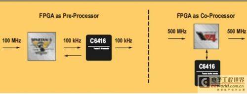
FPGAs can be used with DSP processors as standalone pre-processor (and sometimes post-processor) devices or as coprocessors. In a pre-processing architecture, the FPGA sits directly in the data path and pre-processes the signal, which can then be efficiently and cost-effectively handed off to the DSP processor for lower-rate post-processing.
In a co-processing architecture, the FPGA sits in parallel with the DSP, which offloads specific algorithmic functions to the FPGA to achieve higher processing speeds than the DSP processor alone could achieve. The results of the FPGA processing are passed back to the DSP or to other devices for further processing, transmission, or storage (Figure 1).
The choice between pre-processing, post-processing, or co-processing often depends on the timing margin required to move data between the processor and the FPGA and its impact on overall latency. Although the co-processing solution is the topology most often considered by designers (primarily because the DSP can have more direct control over the data handoff process), it is not always the best overall strategy.
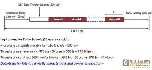
For example, the latest 3G LTE specifications have reduced the transmission time interval (TTI) from 2ms for HSDPA and 10ms for WCDMA to 1ms. This essentially requires less than 1,000?sec of data processing time from the receiver all the way to the MAC layer output. 
Figure 1: FPGA as a pre-processor and co-processor solution
As shown in Figure 2, using an SRIO port on a DSP running at 3.125Gbps (using 8b/10b encoding, and 200 bits of additional overhead for the turbo decoding function) results in a DSP-to-FPGA transmission delay of 230?sec (that is, nearly a quarter of the TTI period is used only to transmit data). Combined with other foreseeable delays, the required turbo codec performance to meet these system timings is up to 75.8Mbps when there are 50 users. 
Figure 2: LTE example of co-processing data transmission delay issues
Using an FPGA to handle the turbo codec as a basically independent post-processor not only eliminates DSP delays, but also saves time because data does not need to be transferred between the DSP and FPGA at high bandwidth. This reduces the turbo decoder throughput to 47Mbps, allowing more economical devices to be selected and reducing system power consumption.
Another consideration is whether to use soft or hard embedded processor IP on Xilinx FPGAs to offload certain system processing tasks, which may further reduce cost, power, and space. With such a large number of signal processing resources, various complex functions (such as those in baseband processing) can be better distributed between DSP processors, FPGA configurable logic blocks (CLBs), embedded FPGA DSP modules, and FPGA embedded processors. Xilinx offers two types of embedded processors: MicroBlaze soft-core processors (commonly used for system control) and higher-performance PowerPC hard-core embedded processors (for more complex tasks). The
advantages provided by FPGA embedded processors allow all non-critical operations to be merged into software running on the embedded processor, thereby minimizing the total amount of hardware resources required for the overall system.
The importance of software and IP
The key question is how to fully unleash this potential. It is necessary to consider what software is needed to abstract the complexity of the problem and what IP can be used, and the FPGA should be considered to provide the best solution for the critical parts.
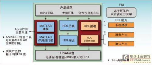
Xilinx is committed to developing industry-leading tools and systems that can achieve efficient FPGA solutions at a higher level of abstraction than HDL tools (such as MATLAB models and C code) can provide. The link from algorithm to silicon can be made as seamless as possible using Xilinx's system generation development tools and AccelDSP synthesis tools specifically for DSP.
There is an increasingly important group of tool providers whose products take development to the electronic system level (ESL) through the C/C++ to logic gate design flow. The purpose of the ESL design tools is to provide a complete system-level approach to generate and integrate the control code for hardware acceleration functions and the processors that control these functions.
No single high-level language or software tool can fit all the different elements seen in today's complex systems. The choice of language and design flow depends on the customer and sometimes on the individual engineer. Therefore, Xilinx has developed a complete set of integrated functions to meet customer needs and provide the best design environment (see Figure 3). 
Figure 3: System-level to FPGA design flow
Summary of this article
In addition, Xilinx is investing heavily in providing a wide range of high-value IP, boards and reference designs to cover many key parts of radio card and baseband applications, including FFT/iFFT, modulation, digital up and down conversion and crest factor reduction circuits.
An example of this focus is the development of industry-leading, high-performance FEC functions, such as turbo encoders and decoders, that are optimized for specific wireless standards and FPGA architectures. As shown in our analysis of 3G LTE latency and turbo decoder traffic requirements, hardware acceleration of FEC functions and their impact on system architecture is an increasingly critical priority in modern wireless device design.
While some expert DSP processors are integrating such functions as embedded modules, it often takes several months from the time the parameters of the FEC function are formulated to meet the new wireless standard to the time the embedded acceleration module appears in silicon. Once embedded, there are still legacy issues and occasional situations where not all functions in the embedded module work as required. At the same time, standards evolve rapidly, and new requirements are occasionally included in the current standards that cannot be supported by fixed embedded modules.
Previous article:Design of infrared moving target recognition and tracking system based on DSP+FPGA
Next article:Design of wireless subsystem based on DSP+FPGA co-processing architecture
- Popular Resources
- Popular amplifiers
- Analysis of the information security mechanism of AUTOSAR, the automotive embedded software framework
- Brief Analysis of Automotive Ethernet Test Content and Test Methods
- How haptic technology can enhance driving safety
- Let’s talk about the “Three Musketeers” of radar in autonomous driving
- Why software-defined vehicles transform cars from tools into living spaces
- How Lucid is overtaking Tesla with smaller motors
- Detailed explanation of intelligent car body perception system
- How to solve the problem that the servo drive is not enabled
- Why does the servo drive not power on?
 Professor at Beihang University, dedicated to promoting microcontrollers and embedded systems for over 20 years.
- LED chemical incompatibility test to see which chemicals LEDs can be used with
- Application of ARM9 hardware coprocessor on WinCE embedded motherboard
- What are the key points for selecting rotor flowmeter?
- LM317 high power charger circuit
- A brief analysis of Embest's application and development of embedded medical devices
- Single-phase RC protection circuit
- stm32 PVD programmable voltage monitor
- Introduction and measurement of edge trigger and level trigger of 51 single chip microcomputer
- Improved design of Linux system software shell protection technology
- What to do if the ABB robot protection device stops
- Analysis of the information security mechanism of AUTOSAR, the automotive embedded software framework
- Brief Analysis of Automotive Ethernet Test Content and Test Methods
- How haptic technology can enhance driving safety
- Let’s talk about the “Three Musketeers” of radar in autonomous driving
- Why software-defined vehicles transform cars from tools into living spaces
- How Lucid is overtaking Tesla with smaller motors
- Wi-Fi 8 specification is on the way: 2.4/5/6GHz triple-band operation
- Wi-Fi 8 specification is on the way: 2.4/5/6GHz triple-band operation
- Vietnam's chip packaging and testing business is growing, and supply-side fragmentation is splitting the market
- Vietnam's chip packaging and testing business is growing, and supply-side fragmentation is splitting the market
- FreeRTOS MPU makes the system more robust!
- Single package, small size drive motor controller is here
- How to debug multiple DSPs?
- Application of 7-inch serial port screen in washing and drying machine
- [RVB2601 Creative Application Development] Bring up the development board and light up the LED
- TI C6000 DSP Notes
- [Chuanglong Technology Allwinner A40i development board] Unboxing experience
- Can OTP be written via communication?
- STM32L0 LL library IIC configuration and usage issues, can't send the data I want. Ask for advice
- Keil C51 cracking problem

 UPC4742G2-A


 京公网安备 11010802033920号