In modern radar receivers, the most widely used structure is the superheterodyne structure. In this structure, the single-chip system often requires an off-chip filter to remove the image signal, such as a SAW filter, which affects the system's integration. In order to achieve a certain image suppression ratio without using an off-chip filter, an image suppression mixer is usually used to provide a suppression degree of about 60 dB. However, modern radar receivers require at least 80 dB of suppression, which increases the difficulty of designing image suppression mixers.
To solve this problem, research work has mainly focused on the design of image suppression LNA. From the literature, it can be seen that through the connection of LNA and notch filter, the suppression degree of the single-chip LNA reaches 20 dB and 75 dB respectively. This paper combines the indicators of LNA in the radar receiver, improves the suppression degree by designing the circuit structure, and achieves a higher image suppression ratio by connecting with the image suppression mixer of the subsequent stage, thereby improving the suppression degree of the entire radar receiver to the image signal.
1 Notch filter
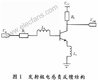
In this paper, the requirements for the low noise amplifier are that the operating frequency band is S band, the noise figure FN is 2-3 dB, the power gain is above 30 dB, the output 1 dB compression point is not less than 10 dBm, and the operating voltage is 5 V. In view of the above requirements, the basic structure of the LNA used is emitter inductor negative feedback. Formula (1) shows that the port can be matched by selecting an appropriate inductance value. Most importantly, this structure avoids noise resistance in the signal channel and greatly reduces the noise figure, as shown in Figure 1.
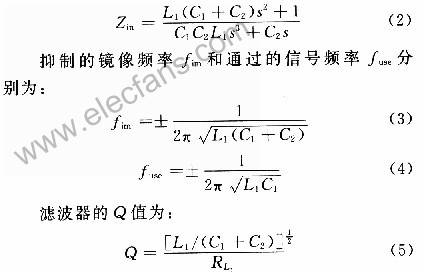
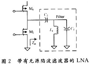
The notch filter is divided into two structures: active and passive. To reduce the complexity of the design, a passive structure is used in the image suppression LNA design, as shown in Figure 2, which includes three passive components: C1, C2 and L1 (the parasitic resistance value in L1 is RL1).
2 LNA Design Analysis
The performance of LNA largely determines the performance index of radar receiver. In order to meet the power gain in the design index, the actual LNA is designed in a three-stage cascade.

Where: Fn, GAn, (IIP3)n are the noise figure (here n=1, 2, 3), power gain and third-order intermodulation parameters of each stage of LNA respectively.
It is not difficult to derive from equations (6) and (7):
(1) Reduce the noise coefficient of the module, mainly reduce the noise coefficient of the previous circuit;
(2) In order to reduce the impact of the noise of the subsequent circuit on the noise of the entire module, the previous module needs to provide appropriate gain;
(3) To improve the linearity of the module, in addition to improving the linearity of each stage of the circuit, the gain of each stage cannot be too high.
In order to meet the noise requirements of the entire LNA, the first-stage amplifier should be mainly designed to optimize the noise to obtain the minimum noise factor. The noise factor of the entire system basically depends on the noise factor of the first stage. The second-stage amplifier should provide a certain gain and linearity while optimizing the noise to avoid the gain of the entire amplifier being too low. The third-stage amplifier is mainly optimized for linearity. By means such as increasing the size of the emitter inductance and the transistor bias current, the output power at the 1 dB power compression point can be effectively increased, but the gain will be affected to a certain extent.
The basic amplifier adopts a common source and common gate structure, which can not only increase the input/output isolation, but also reduce the Miller effect between Ld1 and M2. At the same time, the inductor Ld1 is connected between M1 and M2, which helps to improve the gain and noise of the amplifier.
In the three-stage circuit design, the third stage circuit is the most complicated. The third stage amplifier must meet the requirement that the 1 dB power compression point output is not less than 10 dBm, so it is mainly designed for optimizing linearity. The circuit diagram of the amplifier is shown in Figure 3. The output power third-order intermodulation point of the amplifier can be estimated by equation (8):
From equation (8), we can see that to improve the linearity of the amplifier, we can increase the Vce voltage and collector current Ic of the amplifier tube. Since Vce is not very high, the linearity of the amplifier can be improved mainly by increasing the collector current Ic, but blindly increasing the current will also increase power consumption.
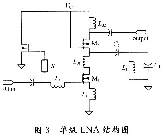
Increasing the emitter inductance can increase the output power at the 1 dB power compression point, but the amplifier gain will decrease, and the input at the 1 dB power compression point will increase, increasing the pressure on the linearity of the previous amplifier. Therefore, the emitter inductance can only be selected to a suitable value and cannot be too large.
3 LNA simulation results
The simulation results are shown in Figures 4 and 5.
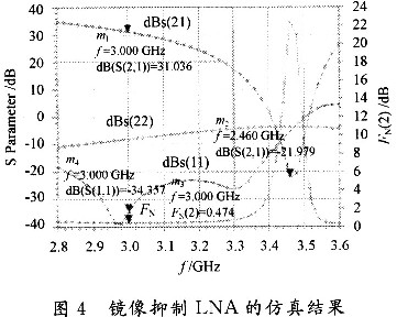
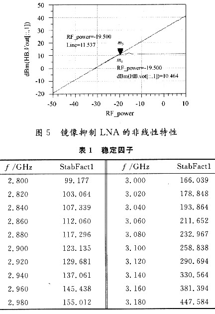
Near the image frequency, the gain drops from about 25 dB without a notch filter to around -21.9 dB, which has a certain inhibitory effect on the image signal entering the LNA. Table 1 shows the stability of the circuit within the frequency band. The coefficient is much greater than 1, and the circuit is absolutely stable.
In addition, it can be seen from equation (5) that the Q value of the notch filter is limited by the parasitic resistance in the inductor. Therefore, in the CMOS process, the characteristics of the inductor affect the final performance of the LNA.
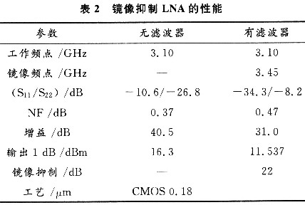
Table 2 shows the comparison of simulation results of LNA with and without notch filters.
4 Conclusion
In order to meet the image suppression requirements of the monolithic radar receiver, a three-stage cascaded image suppression LNA was designed using CMOS 0.18μm technology. By inserting a passive notch filter in the LNA, the image signal is attenuated, thereby reducing the design difficulty of the back-end mixer circuit.
Finally, the designed amplifier was simulated in ADS. The results showed that when the maximum supply voltage was 5 V, the signal frequency band was 3.0-3.2 GHz, the intermediate frequency output was 225 MHz, the power gain was ≥31 dB, the noise figure was ≤0.5 dB, the power of the input/output 1 dB point was -19.5 dBm and 11.5 dBm respectively, and the suppression of the image signal was 22 dB. The use of off-chip filters was avoided, and the system integration was improved. Due to the current CMOS process, the quality of inductors still needs to be improved. If the monolithic image suppression LNA is to achieve better performance, further research is needed.
Previous article:Programmable broadband amplifier based on voltage-controlled gain amplifier VCA822
Next article:Design of microwave low noise amplifier and simulation design with ADS
Recommended ReadingLatest update time:2024-11-16 19:40


- Popular Resources
- Popular amplifiers
-
 Operational Amplifier Practical Reference Handbook (Edited by Liu Changsheng, Zhao Mingying, Liu Xu, etc.)
 -
 A Complete Illustrated Guide to Operational Amplifier Applications (Written by Wang Zhenhong)
 -
 Design of isolated error amplifier chip for switching power supply_Zhang Rui
 -
 DAM medium wave transmitter high frequency power amplifier module test platform_Tian Tian
- High signal-to-noise ratio MEMS microphone drives artificial intelligence interaction
- Advantages of using a differential-to-single-ended RF amplifier in a transmit signal chain design
- ON Semiconductor CEO Appears at Munich Electronica Show and Launches Treo Platform
- ON Semiconductor Launches Industry-Leading Analog and Mixed-Signal Platform
- Analog Devices ADAQ7767-1 μModule DAQ Solution for Rapid Development of Precision Data Acquisition Systems Now Available at Mouser
- Domestic high-precision, high-speed ADC chips are on the rise
- Microcontrollers that combine Hi-Fi, intelligence and USB multi-channel features – ushering in a new era of digital audio
- Using capacitive PGA, Naxin Micro launches high-precision multi-channel 24/16-bit Δ-Σ ADC
- Fully Differential Amplifier Provides High Voltage, Low Noise Signals for Precision Data Acquisition Signal Chain
- Innolux's intelligent steer-by-wire solution makes cars smarter and safer
- 8051 MCU - Parity Check
- How to efficiently balance the sensitivity of tactile sensing interfaces
- What should I do if the servo motor shakes? What causes the servo motor to shake quickly?
- 【Brushless Motor】Analysis of three-phase BLDC motor and sharing of two popular development boards
- Midea Industrial Technology's subsidiaries Clou Electronics and Hekang New Energy jointly appeared at the Munich Battery Energy Storage Exhibition and Solar Energy Exhibition
- Guoxin Sichen | Application of ferroelectric memory PB85RS2MC in power battery management, with a capacity of 2M
- Analysis of common faults of frequency converter
- In a head-on competition with Qualcomm, what kind of cockpit products has Intel come up with?
- Dalian Rongke's all-vanadium liquid flow battery energy storage equipment industrialization project has entered the sprint stage before production
- Allegro MicroSystems Introduces Advanced Magnetic and Inductive Position Sensing Solutions at Electronica 2024
- Car key in the left hand, liveness detection radar in the right hand, UWB is imperative for cars!
- After a decade of rapid development, domestic CIS has entered the market
- Aegis Dagger Battery + Thor EM-i Super Hybrid, Geely New Energy has thrown out two "king bombs"
- A brief discussion on functional safety - fault, error, and failure
- In the smart car 2.0 cycle, these core industry chains are facing major opportunities!
- The United States and Japan are developing new batteries. CATL faces challenges? How should China's new energy battery industry respond?
- Murata launches high-precision 6-axis inertial sensor for automobiles
- Ford patents pre-charge alarm to help save costs and respond to emergencies
- New real-time microcontroller system from Texas Instruments enables smarter processing in automotive and industrial applications
- Sensor selection
- [Atria AT32WB415 series Bluetooth BLE 5.0 MCU] + IAP (Bootloader)
- 【Radio Waves】What is the source of Bluetooth? Does it have any radiation that may affect your health? Is it safe?
- Beetle ESP32-C3 test (Part 3) IDF method to connect to wifi
- Date Spring - Catch the Tail of Spring
- The minimum input voltage of a single-supply VI converter op amp is related to the load
- What are the pull-up and pull-down capabilities of a 0-10V dimmer?
- [ATmega4809 Curiosity Nano Review] Serial Communication
- What is a microcontroller
- Problems with Bluetooth Low Energy modules

 Operational Amplifier Practical Reference Handbook (Edited by Liu Changsheng, Zhao Mingying, Liu Xu, etc.)


 京公网安备 11010802033920号