1 Amplifier Design and Working Principle
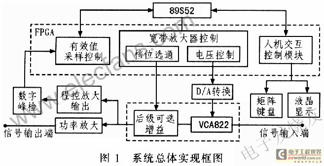
Design a broadband amplifier with AGC function and gain setting through keyboard. The input of the amplifier uses a common-mode amplifier circuit for impedance matching, so that the input resistance reaches the MΩ level. The system design is divided into three modules: broadband amplification, peak sampling, and human-computer interaction.
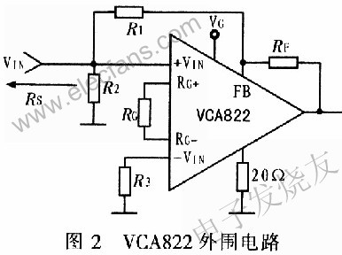
The function of presetting voltage gain in the broadband amplifier module is realized by VCA822. VCA822 is a DC-coupled broadband voltage-controlled gain amplifier with a maximum operating bandwidth of 150 MHz. The amplifier gain is determined by the control voltage and the resistance value of the peripheral resistor. The output of the control voltage is output by the microcontroller to calculate and control the D/A converter, so it can achieve more precise digital control. In addition, the amplifier is connected to a two-speed signal processing circuit, one with a gain of 0 dB and the other with an attenuation gear. Through a control port, the signal can be selected between these two gears. The advantages of this method are clear organization, convenient control, and easy processing by a single-chip microcomputer.
For peak sampling, digital detection is used, that is, the output sinusoidal signal is sampled through a high-speed A/D converter to determine the maximum value of the digital signal collected within a certain period of time, which is the peak value of the signal. However, this general digital peak detection circuit can only work well in the low frequency band. For high-frequency signals required by system design and certain specific frequency signals, certain errors will be generated. Using dual-frequency digital peak detection to sample the signal can effectively avoid errors.
The AGC function is realized on the basis of the above two modules. The voltage value measured by the peak detection is fed back to the single-chip microcomputer, and the single-chip microcomputer realizes precise control of the broadband amplifier circuit. In this way, the peak value of the output signal can be stabilized at about 4.8 V. The overall implementation block diagram of the system is shown in Figure 1.
2 System Hardware Circuit Design
2.1 VCA822 Introduction
The system uses a VCA822 broadband voltage-controlled gain amplifier. Under the control voltage, the device can provide accurate gain and change linearly according to V/V. Its basic gain

2.2 System gain distribution
The fixed gain of the rest of the amplifier is 34 dB, which is provided by the intermediate stage OPA699 and the post-stage power amplifier. During the test, it was found that the control voltage range of VCA822 is -1 to l V, and the device is powered by ±5 V. The peak-to-peak value of the output voltage cannot be greater than 4 V, otherwise the output waveform will be distorted. In order to maximize the dynamic range of the input voltage and realize the adjustable gain of the amplifier, VCA822 is designed as the pre-amplifier, and the gain control is optional at 0 to 24 dB, and the output signal is connected to the in-phase amplifier composed of OPA699. It is controlled by a single-chip microcomputer and selectively cascaded with the two gears of the post-stage. The gains of the two gears are 0 dB and -24 dB respectively. Thus, 9 levels of adjustable gain with a minimum gain of 10 dB and a maximum gain of 58 dB can be achieved.
2.3 Amplifier Circuit
The front-stage input uses MAX477 to design an emitter follower, so that the input resistance approaches infinity, thereby increasing the input impedance. It is coupled with VCA822 through a capacitor, and its control voltage is output by MAX541. Since the conversion range of MAX541 is the same as 0~Vref, a subtractor is added to the output end of the D/A converter, and the output range is -1~+1 V. The reference voltage of MAX541 is provided by MAX6225. The VCA822 is connected to OPA699 in the back stage. OPA699 is a high-gain, high-slew rate broadband operational amplifier. Its operating bandwidth can reach 1 000 MHz. The amplifier with a gain G of 12 is designed using this device, which fully meets the bandwidth requirement of 15 MHz. After that, there is a two-speed attenuation circuit designed through a resistor network and an analog switch, one speed attenuation is 0 dB, and the other speed attenuation is 24 dB, which is controlled by the analog switch MAX333. Finally, the current-type, high-slew-rate operational amplifier AD811 and the post-stage push-pull amplifier designed with discrete components are used to achieve power amplification, with an amplification factor of +4 and increased load capacity. The circuit implementation schematic is shown in Figure 3.
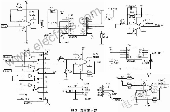
In order to improve the stability of the circuit, this circuit adopts a series of anti-interference measures, including the use of 4.7μF and 104pF capacitors for power supply filtering in the power supply part of each device, the use of shielded wires to connect the signal input and output between amplifiers at each level, and the use of inductors to isolate the digital ground and analog ground.
2.4 Post-stage power amplifier circuit
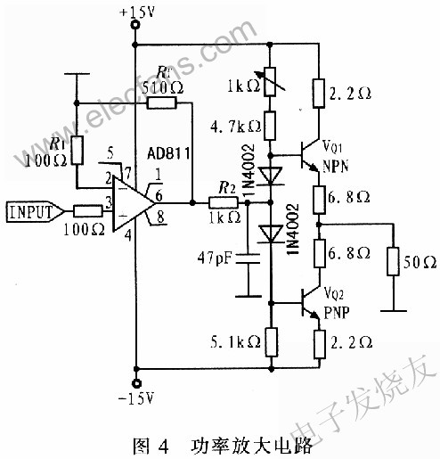
In order to increase the load capacity of the system, considering the limitation of the load driving capacity of the operational amplifier AD811 itself, AD811 is selected here to cooperate with high-frequency small and medium-sized power pair tubes 2N3904 (NPN type) and 2N3906 (PNP type) (the characteristic frequency of the two power tubes fT=300 MHz) to build a 0CL power amplifier. The front stage is composed of AD811 to form a common-phase amplifier with an amplification factor of Av=1+Rf/R3; the back stage uses a power pair tube to expand the current to form a Class A and B power push-pull output form to provide load driving current. According to experimental tests, when the output terminal is connected to a 50 Ω load, the maximum output voltage peak-to-peak value without distortion reaches 18 V. The circuit schematic is shown in Figure 4.
2.5 Digital Detection
The peak detection circuit in this design is based on the signal spectrum shifting theory. Since the A/D converter will have a blind frequency band when sampling at a single sampling rate, the signal is sampled successively at two special frequencies (dual frequencies), and the maximum value in the sampling result can be extracted to obtain the peak value of the periodic signal. This method can take into account both high and low frequencies and is suitable for the system's 100 Hz to 15 MHz situation. Using the A/D converter MAXl97, using two complementary sampling blind areas with sampling rates of f=50.000 kHz and f2=50.005 kHz, a good sampling effect can be obtained. The square wave signal for setting the A/D sampling rate is provided by the FPGA.
3 System Software Design
The system software adopts modular and hierarchical design ideas. With modular design ideas, to control a sub-controller, you only need to call the corresponding control module. Hierarchical design is adopted in the module, and the underlying hardware interface processing is compiled into an independent underlying subroutine, and the processing data is provided upward, and the underlying hardware interface part is shielded from the upper functional module; finally, the main program only needs to call the relevant functional modules to easily build the system.
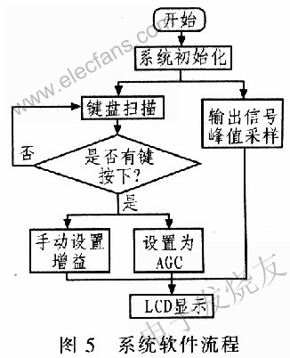
The software part of this system is mainly composed of a single-chip microcomputer, which mainly includes system initialization, interrupt response and interrupt processing. The design function is based on the keyboard key interrupt. By reading the key value entered by the user, the corresponding interrupt response function exchanges data with the corresponding control module in the FPGA in a bus manner, triggering the corresponding control timing in the FPGA to achieve signal amplification and measurement. The system software flow is shown in Figure 5.
4 Data Testing
The system was tested using a digital synthetic signal source, a dual-trace oscilloscope, a simulator, and an AC voltmeter. The frequency of the input signal was adjusted, and the effective value of the output voltage was recorded using an AC voltmeter. The test results show that the amplifier's gain is adjustable in 9 levels within 10 to 58 dB, the -3 dB point is 100 Hz to 15 MHz, and the amplification effect is stable. For the AGC function of the amplifier, the input signal frequency is fixed, the voltage is changed, and when the input signal peak is 9 mV to 1 V, the output signal can be stabilized within the voltage range of 4.5 to 5 V, so the AGC dynamic range is greater than 40 dB. When the amplifier gain is preset to 58 dB, the input terminal is grounded, and the output noise voltage is less than 10 mV.
5 Conclusion
The system design is a controllable gain broadband amplifier with VCA822 as the core. After testing, the system passband is 100 Hz to 15 MHz, the gain is adjustable in 9 levels within 10 to 58 dB, and the dynamic range of the amplifier AGC function is greater than 40 dB. In addition, the system input uses MAX477 to form a common-mode amplifier circuit, so that the system input resistance reaches the MΩ level. The power amplifier circuit built with the post-stage AD811 and discrete components improves the system's load-carrying capacity. The system also adopts a variety of anti-interference measures to effectively ensure the amplifier accuracy and has good noise and linearity.
Previous article:A lock-in amplifier design based on switched capacitor technology
Next article:Design of a three-stage cascaded low noise amplifier
Recommended ReadingLatest update time:2024-11-16 21:53


- Popular Resources
- Popular amplifiers
-
 Operational Amplifier Practical Reference Handbook (Edited by Liu Changsheng, Zhao Mingying, Liu Xu, etc.)
 -
 A Complete Illustrated Guide to Operational Amplifier Applications (Written by Wang Zhenhong)
 -
 Design of isolated error amplifier chip for switching power supply_Zhang Rui
 -
 DAM medium wave transmitter high frequency power amplifier module test platform_Tian Tian
- High signal-to-noise ratio MEMS microphone drives artificial intelligence interaction
- Advantages of using a differential-to-single-ended RF amplifier in a transmit signal chain design
- ON Semiconductor CEO Appears at Munich Electronica Show and Launches Treo Platform
- ON Semiconductor Launches Industry-Leading Analog and Mixed-Signal Platform
- Analog Devices ADAQ7767-1 μModule DAQ Solution for Rapid Development of Precision Data Acquisition Systems Now Available at Mouser
- Domestic high-precision, high-speed ADC chips are on the rise
- Microcontrollers that combine Hi-Fi, intelligence and USB multi-channel features – ushering in a new era of digital audio
- Using capacitive PGA, Naxin Micro launches high-precision multi-channel 24/16-bit Δ-Σ ADC
- Fully Differential Amplifier Provides High Voltage, Low Noise Signals for Precision Data Acquisition Signal Chain
- Innolux's intelligent steer-by-wire solution makes cars smarter and safer
- 8051 MCU - Parity Check
- How to efficiently balance the sensitivity of tactile sensing interfaces
- What should I do if the servo motor shakes? What causes the servo motor to shake quickly?
- 【Brushless Motor】Analysis of three-phase BLDC motor and sharing of two popular development boards
- Midea Industrial Technology's subsidiaries Clou Electronics and Hekang New Energy jointly appeared at the Munich Battery Energy Storage Exhibition and Solar Energy Exhibition
- Guoxin Sichen | Application of ferroelectric memory PB85RS2MC in power battery management, with a capacity of 2M
- Analysis of common faults of frequency converter
- In a head-on competition with Qualcomm, what kind of cockpit products has Intel come up with?
- Dalian Rongke's all-vanadium liquid flow battery energy storage equipment industrialization project has entered the sprint stage before production
- Allegro MicroSystems Introduces Advanced Magnetic and Inductive Position Sensing Solutions at Electronica 2024
- Car key in the left hand, liveness detection radar in the right hand, UWB is imperative for cars!
- After a decade of rapid development, domestic CIS has entered the market
- Aegis Dagger Battery + Thor EM-i Super Hybrid, Geely New Energy has thrown out two "king bombs"
- A brief discussion on functional safety - fault, error, and failure
- In the smart car 2.0 cycle, these core industry chains are facing major opportunities!
- The United States and Japan are developing new batteries. CATL faces challenges? How should China's new energy battery industry respond?
- Murata launches high-precision 6-axis inertial sensor for automobiles
- Ford patents pre-charge alarm to help save costs and respond to emergencies
- New real-time microcontroller system from Texas Instruments enables smarter processing in automotive and industrial applications
- MCU Basics: Detailed explanation of button single click, double click, and long press
- 【McQueen Trial】Main functions corresponding to driver pins
- ti dsp (tms320VC5502) + isp1581 usb2.0 high speed data acquisition solution
- [Problem Feedback] Anlu TD4.6.6-64bit pin constraint input PIN number bank does not automatically update the problem
- Tesla's electric motor
- Design of prison security system by integrating wireless sensors with control network
- Fast charging knowledge sharing: PD protocol fast charging
- [Voice Recognition Positioning] Material Unboxing-ESP32-S2-KALUGA-1
- EEWORLD University ---- The latest version of RTOS training - 15 days to get started with RT-Thread kernel
- [Engineer's Notes] Use 4 "attentions" in PCB wiring to avoid surges!

 Operational Amplifier Practical Reference Handbook (Edited by Liu Changsheng, Zhao Mingying, Liu Xu, etc.)


 京公网安备 11010802033920号