With the rapid development of science and technology, the application of high-resolution mixed analog and digital circuits has been continuously deepened, and the circuit design has become increasingly complex and the accuracy has become higher and higher. Therefore, the design of high-precision AD conversion circuits has become a difficult point for instruments and various measurement and control systems. This system is derived from the temperature control system design of instruments and meters. It uses high-precision, low-temperature drift high-quality analog and digital devices, supplemented by 52 series single-chip microcomputers as controllers, and complex programmable logic devices CPLD (Comp lex Programmable A rray Logi c ) as the hardware platform for frequency testing, realizing the design of high-resolution, low-linear error AD converters. Through this design, you can master the design method of high-precision, low-drift high-end AD converters, the design of CPLD, and the hardware design and software programming of 52 series single-chip microcomputers.
1 System Function and Structure
The main purpose of the system is to design a 16-bit VFC AD converter, which uses the integration principle to convert the input voltage (or current) into frequency output. A CPLD device with a high counting frequency is used to achieve frequency measurement, and the single-chip microcomputer controls the frequency measurement operation and frequency calculation of the CPLD.
To complete AD conversion with V/F converter, one timer and two counters are needed. The counting frequency of the counter limits the increase of the output frequency of the V/F device. This design uses CPLD devices with higher counting frequency and single-chip microcomputer to form a speed measurement module. CPLD has good versatility, avoids dependence on special devices, reduces the risk caused by the discontinuation of special devices or supply problems, and realizes the required control at the same time.
The pulse frequency of the VFC AD converter is proportional to the input voltage. It has high accuracy, good linearity, moderate conversion speed, adjustable conversion bits and speed, minimal connections with the CPU, and increasing the number of conversion bits will not increase the connection with the CPU. Therefore, VFC provides a cheap and effective solution for AD conversion technology.
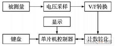
The system can be divided into voltage sampling part, analog-digital conversion part and control part. The voltage sampling part includes: precision test voltage source. The analog-digital conversion part includes: voltage amplification and bias, V/F conversion module, count conversion module. The control part includes: controller module, keyboard, display module. The system principle block diagram is shown in Figure 1.
In order to realize the functions of each module, better solutions were selected: ① precision reference source, precision low temperature drift high-end reference source, voltage division; ② voltage amplification and bias, operational amplifier ICL7650; ③ V / F conversion, using AD652 chip; ④ frequency test, using CPLD (complex programmable logic device); ⑤ controller, using Lingyang's SPEC061A microcontroller; ⑥ display, using LCD screen; ⑦ electrical isolation, using photoelectric coupling. The designed system is shown in Figure 2.

Figure 1 System block diagram

Figure 2 Block diagram of the designed system
2 System Hardware Design
2.1 Precision test reference source
For a 16-bit AD converter, the full-scale input voltage is only 100 mV. If you want to test its performance, you need a reference source with extremely high precision and very low temperature drift. The circuit principle is shown in Figure 3.
AD586 is a high-precision 5 V reference voltage source from AD Company, with a temperature drift as low as 2 10 - 6 /℃ and a noise of 100 nV /Hz. It generates a voltage of 0 to 100 mV by dividing the voltage through fixed resistors and adjustable resistors. In order to increase the voltage load capacity, voltage following is required. OPA333 is a zero-drift precision op amp with a maximum drift of 0.05μV /℃. At the same time, two 2.5 V reference sources LM336 are used to reduce the impact of power supply fluctuations. The output current of LM336 is 10 mA, which can meet the needs of OPA33. The resistor used for voltage division is a pointer type 10-turn adjustable resistor, which can achieve ideal accuracy.

Figure 3 Schematic diagram of reference source circuit
2.2 Voltage amplification and bias
The voltage of 0-100 mV cannot be directly sent to the V/F conversion AD652, but must be precisely amplified and biased to achieve the designed accuracy. The ICL7650 operational amplifier with chopper stabilization function is selected, which can provide low bias current (10pA), bias voltage and relative stability of time and temperature. The input 0-100 mV voltage is amplified 40 times to produce an output of 0-4 V. Because the output frequency of AD652 is also 0 when the input is 0 V, it is difficult to achieve 16-bit accuracy by counting the frequency. Therefore, the DC bias of the input (0-4 V) is set to 1 V, thereby generating a 1-5 V input signal to the AD652; the resistor of the operational amplifier must be selected with 1/1 000 accuracy to ensure the accuracy of the V/F conversion.
The schematic diagram is shown in Figure 4.

Figure 4 Voltage amplification bias principle diagram
2.3 V / F conversion circuit
Voltage/frequency conversion, or V/F conversion, is the process of converting a certain input voltage signal into a frequency signal in a linear proportional relationship. When the input voltage changes, the output frequency also changes accordingly.
This design uses a dedicated integrated chip AD652, supplemented by peripheral circuits to achieve V/F conversion, as shown in Figure 5. AD652 is a high-precision voltage-frequency (V/F) converter launched by ANALOG DEV ICES, USA. It consists of an integrator, a comparator, a precision current source, a monostable multivibrator and an output transistor. Under a ±15 V power supply voltage, the circuit consumes less than 15 mA, its nonlinearity is less than 0.07% when the full scale is 1 MHz, and the optimal temperature stability is ±150 ppm/℃. Using AD652 to achieve V/F conversion can meet higher full-scale frequency response and lower optimal temperature stability.

Figure 5 V /F conversion circuit
Because the full-scale output frequency is set using an external clock, the AD652 can achieve higher linearity and stability. By using the same clock to drive the AD652 and set the counting time gate, the conversion accuracy is independent of the clock frequency and does not change due to changes in the clock frequency.
2.4 Frequency meter circuit based on CPLD
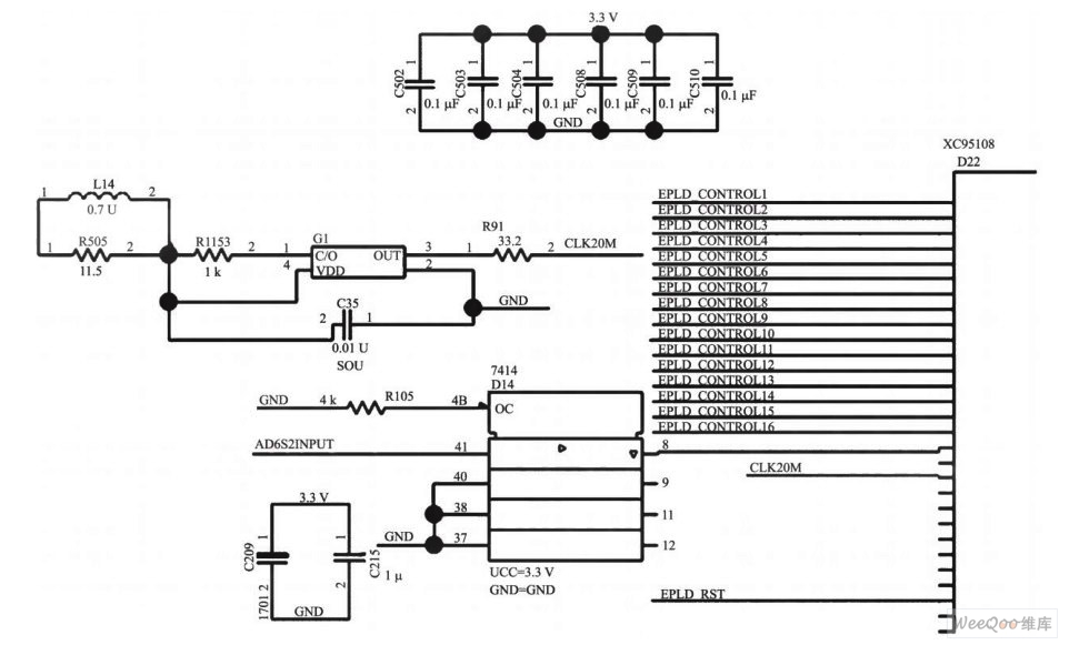
In this system, the CPLD used is the XC95108CPLD (complex programmable logic device) produced by the American company XIL INX. It has 108 macros and 2,400 gates on the chip. The frequency can reach 125 MHz, the delay between pins is 715 ns, and the power supply voltage is 5 V or 313 V. It is an in-system programmable device with more than 64 I/O ports available to users.
XC95108 adopts FLASH programming technology and can be repeatedly erased and written. The designed circuit is shown in Figure 6.
Since the input signal is an AC signal and CPLD (programmable logic device) and Schmitt trigger are digital chips that do not recognize negative signals, the input AC signal needs to be converted into a DC signal, and two resistors are used to implement the voltage clamping function. The clamped signal is shaped into a square wave by 7414 (Schmitt trigger) and directly input into the CPLD to count it.
Since CPLD can achieve high-speed response, accurate counting can be achieved.
The data measured by the frequency meter is the AD conversion result of this system. The conversion accuracy is affected by the reference crystal oscillator and the V/F full-scale range of AD652. Since the reference crystal oscillator of CPLD uses a 20MHz high-precision crystal oscillator, the designed AD conversion frequency is 50kHz, so the number of reference crystal pulses in the counting cycle is 400. The error of CPLD due to random time is only one pulse, and the full-scale frequency of AD652 is high, up to 1MHz, so the accuracy can reach a few thousandths.

Figure 6 Schematic diagram of frequency meter circuit based on CPLD
2.5 Single chip microcomputer control circuit
The control part uses Lingyang SPEC061A microcontroller.
SPCE061A is a 16-bit microcontroller newly launched by Lingyang Technology. Its operating speed range is 0.32-49.152MHz within the operating voltage range of 2.6-3.6V. The higher operating speed makes its application field wider. 2K bytes of SRAM and 32K words of flash ROM only occupy one page of storage space, 32-bit programmable multi-function I/O port; two 16-bit timers/counters; 32 768 Hz real-time clock; low voltage reset/monitoring function; 8-channel 10-bit analog-to-digital conversion input and microphone input with automatic gain control function: dual-channel 10-bit DAC audio output function, etc. SPCE061A is one of the most economical applications of digital sound and speech recognition products.
In this system, SPCE061A mainly realizes functions such as CPLD information reading, keyboard interface and display module control.

Figure 7 MCU structure diagram
2.6 Display interface design
In terms of display, LCD (Liquid Crystal Display) has the following characteristics:
(1) Low operating voltage and low power consumption.
(2) The display is soft and the writing is clear.
(3) Not afraid of strong light exposure. The stronger the light, the greater the contrast and the better the display effect.
(4) Small size, light weight, flat type.
(5) High reliability and long service life.
Therefore, this design uses a 128 × 64 graphic dot matrix LCD to display frequency flow information. The LCD uses 4 lines to display rich information to meet the needs of different users. At the same time, the LCD uses a serial port to transmit data and refreshes the screen once per second, saving the resources of the single-chip computer and laying the foundation for future development and upgrading.
2.7 Other auxiliary anti-interference measures
Generally speaking, the functional design and production of the measurement and control system are not complicated. Functional design is only the starting point of system design. Whether the system can accurately realize these functions during operation is the key to system design. Due to the existence of various interference sources in the actual working environment, these interference sources often have an adverse effect on the reliable operation of the system, and may even cause unexpected events. What's worse is that the entire system is paralyzed and unable to operate, resulting in damage to experimental production equipment and accidents. Therefore, the anti-interference prevention measures of the measurement and control system occupy a pivotal position in the design of the entire system. This design adds hardware anti-interference designs such as coupling circuits, backup power supply monitoring systems, and printed circuit boards to reduce the adverse effects of interference sources on the reliable operation of the system.
3 System Communication Process and Software Implementation
The application software in the system is designed according to the system functional requirements. The general principles are mainly considered from the following aspects:
(1) According to the functional requirements of the software, the system software is divided into several relatively independent parts. According to the connection and time relationship between them, a reasonable overall software structure is designed to make it clear, concise and reasonable in process; (2) Structured programming is adopted, and each functional program is modularized and subroutine. It is convenient for debugging, linking, transplantation and modification; (3) Establish a correct mathematical model. According to the functional requirements, describe the mathematical relationship between each input and output variable, which is an important factor related to the performance of the system; (4) In order to improve the overall efficiency of software design, describe the task in a concise and intuitive way, and draw a program flow chart before writing the application software. This is not only an important part of program design, but also a key part that determines success or failure; (5) Reasonably allocate system resources, among which the most critical is the allocation of on-chip memory. When allocating, its special strengths should be fully utilized to make the best use of it; (6) Strengthen the anti-interference design of the software and improve the reliability of the computer application system. According to the above design principles, the software design adopts a modular structure. The entire software includes modules such as the main program, sampling subroutine, data processing subroutine, and display subroutine.
According to the above principles, the system software program flow chart is designed as shown in Figure 8:

Figure 8 Control program flow chart.
4 Test Results and Analysis
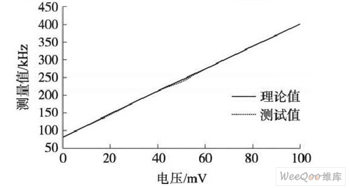
The V/F conversion performance of the designed circuit is tested and the results are shown in Figure 9.

Figure 9 V /F conversion measurement comparison value
Observing through the oscilloscope, 50,000 pulses per second, that is, the conversion frequency is 50 kHz. From the test result chart, it can be seen that this VF conversion meets the requirements of high resolution and low nonlinearity, with a resolution of up to 16 bits, a linear error of <0.2%, and a conversion frequency of up to 50 kHz.
5 Conclusion
This design uses V/F converter to achieve high-resolution AD conversion. It has the characteristics of high full-scale frequency response, low power consumption and low nonlinearity. It is widely used in the temperature control of instruments and meters to meet the requirements for the stability of set temperature control. In the system design, CPLD is used to realize the frequency counting function, which is a method for digital system to accurately measure frequency: count the standard frequency signal and the measured frequency signal at the same time during the sampling time. After the sampling is completed, the count values of the two are compared and multiplied by the standard frequency to get the accurate value of the measured frequency.
Previous article:Design of high-speed and high-precision pipeline analog-to-digital converter
Next article:R.SINθ conversion circuit for multiplying analog input and digital data
Recommended ReadingLatest update time:2024-11-16 22:36


- Popular Resources
- Popular amplifiers
-
 Learn CPLD and Verilog HDL programming technology from scratch_Let beginners easily learn CPLD system design technology through practical methods
 -
 Principles and Applications of Single Chip Microcomputers 3rd Edition (Zhang Yigang)
 -
 Practical Electronic Components and Circuit Basics (4th Edition)_Explanation of basic circuit principles, introduction to electronic components, design of various circuits and practical circuit analysis
 -
 Switching Power Supply Simulation and Design - Based on SPICE (Second Edition)
- High signal-to-noise ratio MEMS microphone drives artificial intelligence interaction
- Advantages of using a differential-to-single-ended RF amplifier in a transmit signal chain design
- ON Semiconductor CEO Appears at Munich Electronica Show and Launches Treo Platform
- ON Semiconductor Launches Industry-Leading Analog and Mixed-Signal Platform
- Analog Devices ADAQ7767-1 μModule DAQ Solution for Rapid Development of Precision Data Acquisition Systems Now Available at Mouser
- Domestic high-precision, high-speed ADC chips are on the rise
- Microcontrollers that combine Hi-Fi, intelligence and USB multi-channel features – ushering in a new era of digital audio
- Using capacitive PGA, Naxin Micro launches high-precision multi-channel 24/16-bit Δ-Σ ADC
- Fully Differential Amplifier Provides High Voltage, Low Noise Signals for Precision Data Acquisition Signal Chain
- Innolux's intelligent steer-by-wire solution makes cars smarter and safer
- 8051 MCU - Parity Check
- How to efficiently balance the sensitivity of tactile sensing interfaces
- What should I do if the servo motor shakes? What causes the servo motor to shake quickly?
- 【Brushless Motor】Analysis of three-phase BLDC motor and sharing of two popular development boards
- Midea Industrial Technology's subsidiaries Clou Electronics and Hekang New Energy jointly appeared at the Munich Battery Energy Storage Exhibition and Solar Energy Exhibition
- Guoxin Sichen | Application of ferroelectric memory PB85RS2MC in power battery management, with a capacity of 2M
- Analysis of common faults of frequency converter
- In a head-on competition with Qualcomm, what kind of cockpit products has Intel come up with?
- Dalian Rongke's all-vanadium liquid flow battery energy storage equipment industrialization project has entered the sprint stage before production
- Allegro MicroSystems Introduces Advanced Magnetic and Inductive Position Sensing Solutions at Electronica 2024
- Car key in the left hand, liveness detection radar in the right hand, UWB is imperative for cars!
- After a decade of rapid development, domestic CIS has entered the market
- Aegis Dagger Battery + Thor EM-i Super Hybrid, Geely New Energy has thrown out two "king bombs"
- A brief discussion on functional safety - fault, error, and failure
- In the smart car 2.0 cycle, these core industry chains are facing major opportunities!
- The United States and Japan are developing new batteries. CATL faces challenges? How should China's new energy battery industry respond?
- Murata launches high-precision 6-axis inertial sensor for automobiles
- Ford patents pre-charge alarm to help save costs and respond to emergencies
- New real-time microcontroller system from Texas Instruments enables smarter processing in automotive and industrial applications
- ADRV9002 Dual Narrow Bandwidth RF Transceiver
- Help, STM32 address data acquisition HardFault_Handler
- CC2640R2 uses the IDE's post-build function to generate a single firmware file
- ST MEMS waterproof pressure sensor LPS27HHW review summary
- The problem of not receiving data when building lorawan gateway with Raspberry Pi
- Two questions about registers
- UWB, Bluetooth, RFID, WIFI and indoor positioning technology
- [NUCLEO-L552ZE Review] + Low Power Measurement Tool
- Lithium battery charging and discharging integrated chip
- Bluetooth module connection problem

 Learn CPLD and Verilog HDL programming technology from scratch_Let beginners easily learn CPLD system design technology through practical methods


 京公网安备 11010802033920号