In modern communication and signal processing systems, high-performance A/D converters are widely used in important design fields such as medical imaging, high-speed data conversion, and QAM modulators as important channels connecting the analog and digital worlds. The comparator is the core unit of the analog-to-digital converter design. Its accuracy, speed, offset voltage, and feedback noise directly affect the overall performance of the system module. The traditional pre-amplifier latch comparator reduces the transmission delay and feedback noise of the comparator by adopting a 3-level or more cascaded pre-amplifier structure, but these indicators are at the expense of higher power consumption and increased chip area. The typical AB type dynamic latch comparator has the characteristics of high speed and low power consumption, but the structure has large feedback noise and offset voltage, which limits the improvement of comparator accuracy. Taking the above factors into consideration, based on the TSMC 0.18μm CMOS standard process, this paper designs a comparator structure that can be applied to high-speed and high-precision A/D converters, gives the theory and method of improving the comparison speed and reducing the feedback noise, and designs and optimizes the circuit based on this.
1 Comparator circuit design
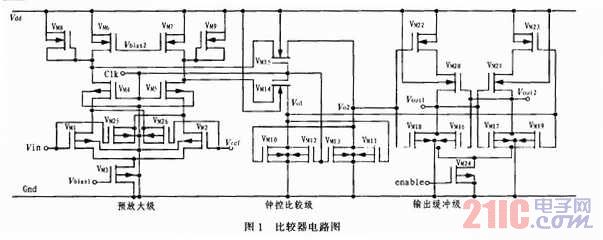
The high-speed and high-precision clock-controlled comparator designed in this paper can be functionally divided into three stages, including pre-amplification stage, clock-controlled comparison stage, and output buffer stage, as shown in Figure 1. The input signal is amplified by the pre-amplification stage circuit, and the amplified signal is transmitted to the clock-controlled comparison stage for regeneration comparison under the control of the clock signal. Finally, the output buffer stage circuit with a positive feedback structure is used to quickly convert the output voltage into a logic level.
1.1 Pre-amplification stage
In order to meet the requirements of high speed and high precision, the design principle of the pre-amplifier is high bandwidth and low gain. The amplifier with MOS diode and current source as load has limited gain-bandwidth product and cannot take into account the requirements of speed and precision at the same time. The hybrid structure of diode and current source load can meet the good compromise of gain and bandwidth.
For the pre-amplification stage in Figure 1, VM1 and VM2 form a differential amplifier tube, and the diode-connected MOS tubes VM8 and VM9 are the active loads of the differential pair. The purpose of adding PMOS mirror current sources VM6 and VM7 is to make part of the input transistor bias current provided by the PMOS current source, so that the transconductance of the load tube can be reduced by reducing the current instead of reducing the width-to-length ratio, thereby improving the differential gain. VM4 and VM5 are clock-controlled switch transistors. When the clock signal clk is at a high level, they form a common source and common gate structure with the input differential pair, improving the circuit's amplification ability for the input signal; when the clock signal clk is at a low level, it can effectively isolate the input signal from the feedback noise of the regeneration node feedthrough, which is very important to ensure the performance of the circuit. The small signal model of the pre-amplification circuit is shown in Figure 2.


From equation (3), it can be seen that the gain and frequency characteristics of the amplifier can be adjusted by reasonably adjusting the aspect ratio of the tube and the current value injected by the current source. It should be noted that in order to meet the response time requirements of the high-speed comparator at the same time, the bandwidth of the pre-amplifier is increased as much as possible while ensuring the gain in the design. The gain and bandwidth simulation results of the pre-amplifier are shown in Figure 3, with a gain of 18.352 dB and a -3 dB bandwidth of 1.122 GHz.

1.2 Clock-controlled comparatives
The speed of the response time of the clock-controlled comparison stage directly affects the speed of the comparator. The principle of this part of the circuit is mainly to use the output of the pre-amplifier to control the change of the voltage at the input end of the comparison stage, that is, to amplify the input difference of the comparator to a value greater than the threshold of the comparison stage through the pre-amplifier circuit, thereby avoiding the non-steady-state output of the comparison stage, thereby regenerating and amplifying the small input voltage difference established at the beginning of the regeneration stage in a short time, and improving the accuracy of the comparator. The interconnection of the two cross-coupled MOS transistors VM10 and VM11 of the clock-controlled comparison stage (Figure 1) realizes the purpose of improving the gain of the comparison stage circuit by using a positive feedback loop structure. The switching transistors VM4, VM5, VM12, VM13, VM14, and VM15 jointly control the working state of the comparison stage. The speed of state conversion affects the regeneration speed of the comparison stage. The response time of the MOS switch is
![]() , so the regeneration time of the comparison stage can be shortened by reducing the size of the transistor. The switching transistors in this design all use the minimum size under this process.
, so the regeneration time of the comparison stage can be shortened by reducing the size of the transistor. The switching transistors in this design all use the minimum size under this process.
The comparison circuit has two working modes: reset mode and comparison mode. When the clock signal clk is high, VM4 and VM5 are turned on to enable the preamplifier to collect and amplify the input signal, VM12 and VM13 are turned on and VM14 and VM15 are turned off to force the regeneration node voltages Vo1 and Vo2 to a low level. When the clock signal clk is low, VM4, VM5, VM12, and VM13 are turned off, VM14 and VM15 are turned on, and the system enters the comparison mode. The difference in gate-source voltage between VM10 and VM11 will result in different currents flowing through the two transistors, and the voltages of the two regeneration nodes Vo1 and Vo2 will rise at different speeds. The end with a faster voltage rise will suppress the rise of the regeneration node voltage at the other end, and the positive feedback mechanism of the comparison circuit will rapidly increase the voltage difference of the regeneration node.
1.3 Output Buffer Stage
At present, the comparator in the A/D converter usually makes comparison at the transition edge of the clock. The circuit designed in this paper is realized by adding an output buffer stage (also called post-amplifier stage) after the comparison stage circuit - a positive feedback latch structure, whose main function is to convert the output signal of the comparison stage circuit into a logic level (0V or 5V).
When the enable signal enable is low, VM24 is turned off (Figure 1), the regeneration node voltage cannot act on the output buffer stage circuit, and the entire comparison system is in an inoperative state. When enable is high, VM24 is turned on, and the output buffer stage circuit is turned on. When the clock signal clk is low, VM18 and VM19 are turned on, and VM16, VM17, VM20, and VM21 form an end-to-end amplifier, which quickly converts the comparator's output voltages VOUT1 and VOUT2 into full-swing digital levels according to the different regeneration node voltages of the comparison stage. When clk is high, VM18 and VM19 are turned off, and the buffer stage circuit enters the state of latching the output signal, ensuring the stability of the output result.
2 Analysis and optimization of circuits
2.1 Comparison speed
When the clock signal clk is at a low level, the clock-controlled comparison stage circuit enters a regeneration phase. At this time, the small signal model of this part of the circuit is shown in FIG4 .

According to the node current of the small signal model, the following formula can be obtained:

Where C1 and C2 are the capacitors from the drain of VM10 and VM11 to ground, R1 and R2 are the resistors from the drain of VM10 and VM11 to ground, and
![]() τ is the initial voltage applied to the regeneration node. τ is the time constant. Assuming that all transistors are the same, then R1=R2, C1=C2, gm11=gm10=gm, and thus τ1=τ2=τ.
τ is the initial voltage applied to the regeneration node. τ is the time constant. Assuming that all transistors are the same, then R1=R2, C1=C2, gm11=gm10=gm, and thus τ1=τ2=τ.
△Vo is used to define the difference between Vo1 and Vo2, and △Vi is used to define
![]() the difference between , so
the difference between , so
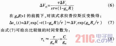
It should be noted that: 1) before the clock-controlled comparison stage is enabled, the speed of the voltage change of the regeneration node increases with the increase of △Vi; 2) the smaller the absolute value of τ, the smaller the transmission delay, and the faster the comparator works. It can be seen that the speed of the comparator can be increased by increasing the input transconductance, reducing the load capacitance of the output node, and increasing the initial input voltage difference.
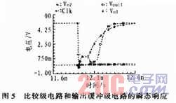
In addition, the output buffer circuit added after the comparison circuit can also shorten the comparison time of the comparator. Its advantage is that it combines the positive exponential response of the comparison circuit and the negative exponential response of the positive feedback latch structure, that is, the comparison circuit first amplifies the input signal to a certain difference Vx after a period of time, and the output buffer circuit will quickly convert the output voltage of the comparator to a logic level. The transient response of the comparison circuit and output buffer circuit designed in this paper is shown in Figure 5.
2.2 Feedback Noise
During the working phase of the comparison circuit, the rapid change of the regeneration node voltage causes interference to the input signal through parasitic capacitance, which is called feedback noise, which seriously affects the accuracy of the comparator. A large number of comparators are used in analog-to-digital converters, and the feedback noise on these comparators will increase the bit error rate of the ADC. In order to effectively suppress the impact of feedback noise on the comparator, this paper adopts isolation and complementary technology.
Switching transistors VM4 and VM5 are added to the pre-amplifier stage to isolate the input signal from the feedback noise of the regeneration node voltage. When the comparator changes from the reset stage to the comparison stage, VM 4 and VM5 are turned off, cutting off the signal path between the pre-amplifier and the comparison stage circuit, so that the rapid change of the regeneration node voltage cannot be directly coupled to the input of the comparator, thereby reducing the feedback noise.
The specific implementation method of complementary technology is to add the capacitor composed of NMOS tubes VM25 and VM26 at the input end of the pre-amplifier stage, so that it forms a complementary structure with the gate-drain capacitance CGD of the input transistors VM1 and VM2. In order to achieve the best complementary effect, the values of CM25 and CM26 should be equal to CGD, that is, the width of VM25 and VM26 should be half of VM1 and VM2. When the voltage at the source end of the input pair changes, the complementary structure composed of CM25, CGD-M2 and CM26, CGD-M1 makes the changing currents offset each other, thereby improving the stability of the input voltage.
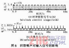
When the comparator clock frequency is 300 MHz and the input signal amplitude is 100 mV, the peak jitter of the comparator reference signal caused by feedback noise is within 5 mV, as shown in Figure 6. Compared with the feedback noise of the typical AB type latch comparator of about 100 mV, the comparator circuit structure designed in this paper has a stronger ability to suppress feedback noise.
3 Simulation Results
In the Cadence software platform, the Specte tool is used to simulate the comparator circuit based on the TSMC 0.18μm CMOS standard process model. Using a 5 V power supply voltage, a 300 MHz clock frequency, and a reference voltage Vref that is always kept at 1.8 V, the transient response of the circuit is shown in Figure 7.
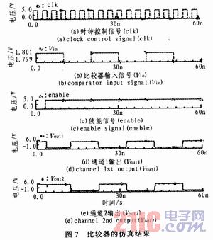
The first column is the clock control signal clk; the second column is the comparator input signal Vin, Vin is connected to a rectangular pulse with positive and negative levels of 1.801 V and 1.799 V; the third column is the enable signal enable; the fourth and fifth columns are the waveforms of the comparator output nodes Vout1 and Vout2. The curve in Figure 7 shows that when the enable signal is high, the comparator works and compares the size of Vin and Vref at the falling edge of the clock signal clk, and latches the output result at the rising edge of clk. When Vin is 1 mV larger than Vref, the output voltage Vout1 is low and Vout2 is high, otherwise the output result is opposite. The simulation results meet the design requirements, and the comparator can achieve a comparison accuracy of 10 bits.
Due to the influence of factors such as process and temperature changes, the actual device parameters will have certain variability. In order to improve the product yield and actual performance indicators, the circuit was simulated at 27, -40 and 100 ° C. Under different process corners, the comparator can work normally, and its main performance parameters such as transmission delay, power consumption and input common mode range fluctuate within a certain range, as shown in Table 1.

4 Conclusion
Based on the pre-amplifier latch theory, this paper designs a high-speed and high-precision clock-controlled voltage comparator. The pre-amplifier stage, clock-controlled judgment stage and output buffer stage structure are used to achieve high comparison speed and obtain a smaller resolvable voltage. The theory and method of improving the comparison speed and feedback noise of the comparator are analyzed in detail. Under the TSMC 0.18μm CMOS standard process, a comprehensive simulation of possible process deviations and changes in operating temperature is carried out. The simulation results show that the clock-controlled comparator has significant advantages in important performance parameters such as speed, accuracy, transmission delay and feedback noise, and can be applied to the design of high-speed and high-precision analog-to-digital converters and analog IP cores.
Previous article:System Design and Implementation of Switched Capacitor Filter
Next article:Basic knowledge and applications of insulated gate bipolar transistors
Recommended ReadingLatest update time:2024-11-17 01:37

- High signal-to-noise ratio MEMS microphone drives artificial intelligence interaction
- Advantages of using a differential-to-single-ended RF amplifier in a transmit signal chain design
- ON Semiconductor CEO Appears at Munich Electronica Show and Launches Treo Platform
- ON Semiconductor Launches Industry-Leading Analog and Mixed-Signal Platform
- Analog Devices ADAQ7767-1 μModule DAQ Solution for Rapid Development of Precision Data Acquisition Systems Now Available at Mouser
- Domestic high-precision, high-speed ADC chips are on the rise
- Microcontrollers that combine Hi-Fi, intelligence and USB multi-channel features – ushering in a new era of digital audio
- Using capacitive PGA, Naxin Micro launches high-precision multi-channel 24/16-bit Δ-Σ ADC
- Fully Differential Amplifier Provides High Voltage, Low Noise Signals for Precision Data Acquisition Signal Chain
- Innolux's intelligent steer-by-wire solution makes cars smarter and safer
- 8051 MCU - Parity Check
- How to efficiently balance the sensitivity of tactile sensing interfaces
- What should I do if the servo motor shakes? What causes the servo motor to shake quickly?
- 【Brushless Motor】Analysis of three-phase BLDC motor and sharing of two popular development boards
- Midea Industrial Technology's subsidiaries Clou Electronics and Hekang New Energy jointly appeared at the Munich Battery Energy Storage Exhibition and Solar Energy Exhibition
- Guoxin Sichen | Application of ferroelectric memory PB85RS2MC in power battery management, with a capacity of 2M
- Analysis of common faults of frequency converter
- In a head-on competition with Qualcomm, what kind of cockpit products has Intel come up with?
- Dalian Rongke's all-vanadium liquid flow battery energy storage equipment industrialization project has entered the sprint stage before production
- Allegro MicroSystems Introduces Advanced Magnetic and Inductive Position Sensing Solutions at Electronica 2024
- Car key in the left hand, liveness detection radar in the right hand, UWB is imperative for cars!
- After a decade of rapid development, domestic CIS has entered the market
- Aegis Dagger Battery + Thor EM-i Super Hybrid, Geely New Energy has thrown out two "king bombs"
- A brief discussion on functional safety - fault, error, and failure
- In the smart car 2.0 cycle, these core industry chains are facing major opportunities!
- Rambus Launches Industry's First HBM 4 Controller IP: What Are the Technical Details Behind It?
- The United States and Japan are developing new batteries. CATL faces challenges? How should China's new energy battery industry respond?
- Murata launches high-precision 6-axis inertial sensor for automobiles
- Ford patents pre-charge alarm to help save costs and respond to emergencies
- Five Design Challenges Facing Remote Patient Monitoring Systems
- 【FAQ】ST wide bandgap high-performance silicon carbide and gallium nitride products and technologies and different application cases
- Answer the questions to win a gift | Choose gate drivers from Infineon, and get a 50-yuan JD card
- Share a table of the electrical and thermal characteristics of the selected packaging materials
- [RVB2601 Creative Application Development] Flower Watering Detector - Development Board Introduction
- Come if you dare | Infineon IGBT7 escape room, you are invited to play!
- Does anyone have MRF6S19100H_MDL_ADS suitable for ADS2019?
- CC2541 Mini Development Kit User Experience Sharing + my love
- There are several problems when ADC samples two sets of DAC output voltages, as shown in the figure. In addition, if the signal is about 1uA, does it need 20 bits?
- The difference between CSS SSC selectors with and without spaces

 A low-latency and low-power PWM comparator circuit design


 京公网安备 11010802033920号