Introduction
Instrumentation amplifiers (IAs) are powerful and versatile when interfacing with sensors, but they also have some limitations that hinder the design of variable-gain IAs or programmable-gain instrumentation amplifiers (PGIAs). In some literature, the latter are also referred to as software-programmable-gain amplifiers (SPGAs). Such PGIAs are needed because there are often situations where the circuit needs to be adjusted to a wide range of sensor or environmental conditions. With fixed gain, system designers may have to deal with suboptimal SNR, which reduces accuracy. My colleague published the Analog Dialogue article, “ Programmable-Gain Instrumentation Amplifiers: Finding the Right One ,” which discusses a number of techniques that can help create a precise and stable PGIA. The article points out the possible pitfalls of such a design and presents a comprehensive survey of available solutions and techniques. In this article, I will introduce another tool and method to facilitate this work, and I will walk through each design step to quickly grasp the external component values required to create a precision PGIA using a newly released instrumentation amplifier.
A New Instrumentation Amplifier Architecture
A common instrumentation amplifier architecture is shown in Figure 1.

Figure 1. Classic instrumentation amplifier
The gain is set by the value of the external resistor, RG. To create a PGIA using this type of device, simply switch the value of RG. This switching is typically accomplished using an analog switch or multiplexer. However, this task is complicated by some nonideal behaviors of analog switches—such as the on-resistance of the switch, the capacitance of the channel, and the variation of the channel resistance with applied voltage.
A variation on the standard instrumentation amplifier structure is shown in Figure 2. Note how the RG pins are broken out into ±RG,S and ±RG,F, individually brought out and configured externally from the device package.
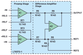
Figure 2. The LT6372-1 architecture allows configuration of some IA internal nodes
The architecture shown in Figure 2 has an important practical feature: the ability to configure the instrumentation amplifier so that it can switch between several different gain values while minimizing the gain error caused by the switch resistance. This feature can be used to create a PGIA.
As mentioned above, any resistor-programmable instrumentation amplifier can have its gain changed by switching the value of the gain resistor. However, this approach has significant disadvantages, such as:
The nominal value of the switch on-resistance (RON) and its variations can cause large gain errors.
High gain values may not be achievable due to the lower switch RON values required.
Switching nonlinearity can cause signal distortion. This is because the signal current flows directly through RON, so any change in its value with voltage will cause distortion.
When the LT6372-1 is configured as a PGIA, these issues can be mitigated because the RG,F and RG,S pins are brought out separately, as shown in Figure 3. In this schematic, the signal generated by the Wheatstone bridge (composed of R5 to R8) is amplified to provide 4 possible gain values, which can be selected by the user based on the selected SW1 switch position. Using the LT6372 family pinout, we can create a PGIA to obtain the desired gain value by changing the RF/RG ratio.
Additionally, the U1, U2 analog switch RON, a source of gain error, is minimized because it can be placed in series with the input stage inverting port and its feedback resistor. Configured in this way, RON is a small fraction of the total internal 12.1 kΩ feedback resistor and has little effect on gain error and drift. Likewise, because RON is a small fraction of the total feedback resistor, changes in its value over voltage have little effect, so distortion due to switch nonlinearity is minimized. Additionally, the input stage of this device consists of a current feedback amplifier (CFA) architecture, which inherently allows for less bandwidth or speed changes when gain is changed than traditional voltage feedback amplifiers. 1 All of these factors combined allow the creation of a precision PGIA with precise gain steps using low-cost external analog switches.
1 The CFA closed-loop bandwidth is inversely proportional to the value of RF, while the traditional voltage feedback architecture bandwidth is inversely proportional to the gain (RF/RG).
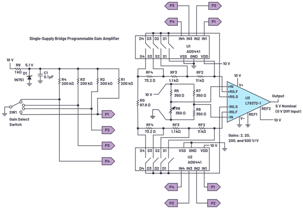
Figure 3. LT6372-1 PGIA bridge interface with four gain settings
Figure 4 shows a simplified diagram of the PGIA, showing how different taps of the resistor ladder (implemented by a total of eight analog switches, shorted two at a time to set the gain) configure the circuit. In this figure, two switch banks are described by one of the four possible gain values; the –RG,S and +RG,S pins are shorted to the RF3/RF4 junction.

Figure 4. Block diagram of the LT6372-1, with simplified external connections for the PGIA (gain switches not shown)
Design steps for calculating the gain of external resistors
Figure 3 shows the complete PGIA configuration, including the necessary switches, which can accommodate any size gain range. Four possible gain values are included, but this can be increased by adding more switches to the design. As mentioned earlier, the ability to configure the RG,F and RG,S pins allows us to increase RF to increase gain and decrease RG to decrease gain to create a very versatile PGIA. To calculate the gain, we can calculate the feedback resistance as the internal 12.1 kΩ adjustment resistor plus the additional resistance in series with RG,F on the RG,F to RG,S port connection. Conversely, the gain setting resistance is the total resistance between +RG,S and -RG,S. To summarize:
RF = 12.1 kΩ + the resistors between RG,F and RG,S on each of the two input amplifiers
RG = resistance between +RG,S and –RG,S
In this configuration, the possible range of gain is 1 V/V to 1000 V/V. When the switches on both U1 and U2 are set to short pins S3 and D3, the corresponding RF and RG values, and the resulting gain, are as follows:
RF = 12.1 kΩ + 11 kΩ + 1.1 kΩ = 24.1 kΩ
RG = 73.2 Ω + 97.6 Ω + 73.2 Ω = 244 Ω
G = 1+ 2RF/RG = 1 + 2 × 24.1 kΩ/244 Ω = 199 V/V
It is easy to see that deciding which values of external resistors to use is an iterative and interdependent process, with the possible gain values interacting to influence the resistors chosen. For ease of reference, some common gain value combinations are listed in Table 1, however, many other gain combinations (G) are possible.
Table 1. Component values for some PGIA gain combinations

Steps to determine the value of PGIA
We can use the formula in Equation 1 to sequentially calculate the value of the individual resistors in the gain network. The way this equation determines the resistors is shown in Figure 3, and Case 2 in Table 1 (gains of 2, 20, 200, and 500 V/V) is used as an example of the calculation. The feedback resistors interact with the gain setting resistors; therefore, the formula must be a series where the current term depends on the previous term. Calculation
The formula is as follows:

Here are some definitions:
RF1 = 12.1 kΩ (internal resistor of LT6372-1)
M: Gain quantity (4 for this circuit)
Gi: Gain example (in this example, G1 – G4 are 2, 20, 200, or 500 V/V respectively)
i: varies between 1 and (M-1), used to calculate RFi+1

Equation 1 can be used to calculate the required feedback resistor for any gain combination. A dummy variable (j) acts as a counter to keep a running count of the previous feedback resistors.
Before doing any calculations, it is recommended to draw a resistor network similar to the one shown in Figure 3. There are (2 × M) – 1 resistors in this network, where M = the number of gains. In this example, M = 4, so there will be 7 resistors in the string. Equation 1 needs to be evaluated for i = 1 → (M – 1).
G1 = 2, G2 = 20, G3 = 200, G4 = 500 V/V
According to equation 2:

According to i = 1 → (M-1), the value of equation 1 is iteratively evaluated.
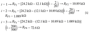
The center resistance RG can then be calculated using the following equation:

After this final calculation, all four resistor values in Table 1 are calculated and the design is complete.
Measured performance graph
These graphs show the performance that can be achieved using this PGIA configuration:
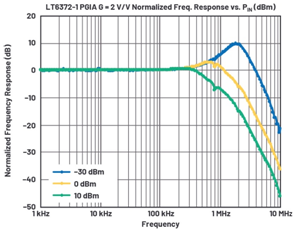
Figure 5. PGIA large signal frequency response
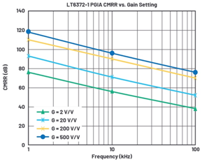
Figure 6. PGIA CMRR vs. frequency
The switch capacitance of the ADG444 causes some noticeable peaking in the small signal frequency response at the lowest gain setting (G1 = 2 V/V) (see Figure 7). This phenomenon only occurs at lower gain settings because the bandwidth of the LT6372-1 extends enough to be affected by the pF capacitance of the switches. Solutions to this side effect include selecting switches with lower capacitance (such as the ADG611/ADG612/ADG613 with 5 pF capacitance) or limiting the lowest gain setting of the PGIA.

Figure 7. PGIA small signal low gain peaking
in conclusion
This article describes how to add a gain selection function to an instrumentation amplifier using the pinout of the newly released LT6372 family of devices. The characteristics of this PGIA are analyzed and its design steps are detailed along with performance measurements. The LT6372-1 is well suited for this type of solution due to its high linearity and precise dc specifications and performance.
About the Author
Hooman Hashemi joined Analog Devices in March 2018 and is engaged in application development for new product specification testing and product features and uses. Hooman previously worked at Texas Instruments for 22 years as an applications engineer focusing on high-speed product lines. He graduated from Santa Clara University in August 1989 with a master's degree in electrical engineering and from San Jose State University in December 1983 with a bachelor's degree in electrical engineering. Contact: hooman.hashemi@analog.com.
Previous article:New version of classic instrumentation amplifier (PGIA) offers greater design flexibility
Next article:Sample and Hold Amplifier
Recommended ReadingLatest update time:2024-11-15 08:10


- Popular Resources
- Popular amplifiers
-
 Design of isolated error amplifier chip for switching power supply_Zhang Rui
 -
 DAM medium wave transmitter high frequency power amplifier module test platform_Tian Tian
 -
 Integrated operational amplifier
 -
 Electrical and Electronic Technology (Editors-in-Chief: Liu Yaoyuan, Hu Minshan; Associate Editors-in-Chief: Zou Xiaolian, Zhou Hongyu, Li Heshui)
- High signal-to-noise ratio MEMS microphone drives artificial intelligence interaction
- Advantages of using a differential-to-single-ended RF amplifier in a transmit signal chain design
- ON Semiconductor CEO Appears at Munich Electronica Show and Launches Treo Platform
- ON Semiconductor Launches Industry-Leading Analog and Mixed-Signal Platform
- Analog Devices ADAQ7767-1 μModule DAQ Solution for Rapid Development of Precision Data Acquisition Systems Now Available at Mouser
- Domestic high-precision, high-speed ADC chips are on the rise
- Microcontrollers that combine Hi-Fi, intelligence and USB multi-channel features – ushering in a new era of digital audio
- Using capacitive PGA, Naxin Micro launches high-precision multi-channel 24/16-bit Δ-Σ ADC
- Fully Differential Amplifier Provides High Voltage, Low Noise Signals for Precision Data Acquisition Signal Chain
- LED chemical incompatibility test to see which chemicals LEDs can be used with
- Application of ARM9 hardware coprocessor on WinCE embedded motherboard
- What are the key points for selecting rotor flowmeter?
- LM317 high power charger circuit
- A brief analysis of Embest's application and development of embedded medical devices
- Single-phase RC protection circuit
- stm32 PVD programmable voltage monitor
- Introduction and measurement of edge trigger and level trigger of 51 single chip microcomputer
- Improved design of Linux system software shell protection technology
- What to do if the ABB robot protection device stops
- CGD and Qorvo to jointly revolutionize motor control solutions
- CGD and Qorvo to jointly revolutionize motor control solutions
- Keysight Technologies FieldFox handheld analyzer with VDI spread spectrum module to achieve millimeter wave analysis function
- Infineon's PASCO2V15 XENSIV PAS CO2 5V Sensor Now Available at Mouser for Accurate CO2 Level Measurement
- Advanced gameplay, Harting takes your PCB board connection to a new level!
- Advanced gameplay, Harting takes your PCB board connection to a new level!
- A new chapter in Great Wall Motors R&D: solid-state battery technology leads the future
- Naxin Micro provides full-scenario GaN driver IC solutions
- Interpreting Huawei’s new solid-state battery patent, will it challenge CATL in 2030?
- Are pure electric/plug-in hybrid vehicles going crazy? A Chinese company has launched the world's first -40℃ dischargeable hybrid battery that is not afraid of cold
- It is said that uC/OS system is free. Is it true?
- Last two days! Free review - Pingtouge scenario-based Bluetooth Mesh gateway development kit
- EEWORLD University Hall----Research and development of high-speed motors
- How to choose between different chips in TI's Sub-1GHz product line?
- Why does C6000 need Cache?
- What are the benefits of using an op amp to drive a MOS tube? Who knows? Tell me
- How to convert Allegro PCB to AD PCB?
- PIC32MK encounters problems in UART data transmission and reception using DMA
- Recruiting part-time motor modeling training teachers
- Add a wireless zoom function to your phone

 Design of isolated error amplifier chip for switching power supply_Zhang Rui


 京公网安备 11010802033920号