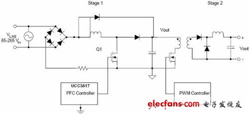
PFC offline power converter systems are usually designed as a two-stage cascade. The first stage is a boost converter because this topology has continuous input current (current waveform control can be achieved by using a multiplier) and average current mode control that can achieve a near-unity power factor. However, the boost converter requires an output voltage that is higher than the input voltage and another converter to step down the output voltage to a usable voltage level (see Figure 1).

Figure 1. Typical two-stage off-line power converter
Advantages of Boost Follower
The fixed output voltage of a conventional boost converter is much higher than the maximum peak line voltage. However, since a step-down converter can be designed to handle voltage variations, there is no need for special regulation or regulation of the boost voltage. As long as the boost voltage is above the peak input voltage, the converter will operate properly. Varying the boost voltage as the peak line voltage varies has the following advantages (e.g., boost follower pre-regulator): first, a smaller size of the boost inductor, and second, lower switching losses during low-voltage operation. Figure 2 shows the output voltage variation of a boost follower and a conventional PFC pre-regulator as the input voltage (Vin(t)) varies.

Figure 2. Changes in output voltage of a conventional boost regulator and a boost follower as input voltage changes.
Lower boost inductance (L)
The boost inductor selection is based on the maximum allowable ripple current (ΔI) when both the line voltage (Vin(min)) and the output voltage (Vout(min)) are at their minimum and the duty cycle (D) is at its maximum. The following equation is used to calculate the required inductance for the boost power stage of the prototype power supply. A reduction in the minimum output voltage peak results in a reduction in the maximum duty cycle, which in turn reduces the boost inductance.
Lower boost switching losses during low voltage operation
In an offline PFC converter, most of the power consumption of the converter comes from the switching losses when performing the boost switch transition (Q1). The following equations can calculate the FET switching losses (PFE_TR) and part of the FET parasitic capacitance losses (PCOSS). In the following equations, IRMS_L represents the rms current flowing through the boost inductor, Ton and Toff are the number of FET switching transitions, the variable fs represents the switching frequency of the power converter, and Coss represents the FET parasitic capacitance. From the equations, it can be deduced that if the output voltage is reduced, the switching losses will also be reduced. The output voltage of the boost follower PFC converter is much lower than the output voltage of the traditional PFC boost converter when operating at low voltage, which also reduces the switching losses.
To further illustrate, we built two 250W converter prototypes using the UCC3817 PFC control IC for universal line voltages (e.g., 85Vac to 265Vac). One converter design uses a conventional topology with an output voltage of 390V. The other converter is built using boost-follower technology with an output voltage that can vary from 230V to 387.5V. The boost-follower power is about 2%~3% higher when operating at low voltages. See Figure 3 for a power comparison.

Figure 3 Efficiency of conventional PFC and boost follower PFC at 85Vrms
Additional Circuitry Required
Designing a boost-follower PFC power stage with a typical PFC controller is not difficult and requires only five additional electronic components (see Figure 4).

Figure 4: The boost follower circuit only requires five more components
The additional electronic components required are C1, R1, R2, R4, Q1 and D1, which are used to absorb the additional current of the voltage amplifier inverting signal in the voltage loop feedback. When the rectified line voltage increases or decreases, Q1 draws a corresponding current through R3, causing the output voltage to change with the line voltage. The diode is used to offset the change in Q1 base emitter junction temperature (Vbe). Capacitor C1 and R2 form a low-pass filter to eliminate the ripple voltage caused by the rectified line voltage.
Application Examples
This circuit is designed to vary the output voltage from 230V to 390V, which is roughly a 2:1 input range. In the final design, the output voltage should be within 8% of the design voltage as the line voltage increases. In addition to the resistor tolerance and variations in the base-emitter voltage (Vbe) of Q1, the forward voltage of the diode is also a source of error. In this application, the boost voltage does not need a tight tolerance because the downstream converter will correct for any unusual changes in the PFC pre-regulator output voltage.
The first step in designing this circuit is to build the voltage divider, which can be formed by R3 and R4. First select R3, then use the following equation to calculate the required value for R4. In this design, the value of Vref is 7.5V and the value of Vout (minimum) is 230V.
The voltage divider formed by R1 and R2 is used to vary the base voltage of Q1 between 1.4V and 3.9V. Care must be taken not to saturate the transistor. The following equation can be used to select the value of R2:
Vqb1(min) is the base voltage of Q1 when the input voltage is minimized to 85 V rms. Vd is the forward diode voltage drop of the circuit.
Capacitor C1 is used to filter out the rectified line voltage ripple. To limit the third-order harmonic current distortion, a filter is installed to reduce the rectified line frequency to 1.5% of the maximum voltage at the Q1 base point (Vqb1(max)).
In this design, the maximum input voltage is 265V and the line frequency (f_line) is 60Hz.
Previous article:Realization of Resonance Elimination in Power System
Next article:How to reasonably design the switching power supply
- Popular Resources
- Popular amplifiers
- High signal-to-noise ratio MEMS microphone drives artificial intelligence interaction
- Advantages of using a differential-to-single-ended RF amplifier in a transmit signal chain design
- ON Semiconductor CEO Appears at Munich Electronica Show and Launches Treo Platform
- ON Semiconductor Launches Industry-Leading Analog and Mixed-Signal Platform
- Analog Devices ADAQ7767-1 μModule DAQ Solution for Rapid Development of Precision Data Acquisition Systems Now Available at Mouser
- Domestic high-precision, high-speed ADC chips are on the rise
- Microcontrollers that combine Hi-Fi, intelligence and USB multi-channel features – ushering in a new era of digital audio
- Using capacitive PGA, Naxin Micro launches high-precision multi-channel 24/16-bit Δ-Σ ADC
- Fully Differential Amplifier Provides High Voltage, Low Noise Signals for Precision Data Acquisition Signal Chain
- Innolux's intelligent steer-by-wire solution makes cars smarter and safer
- 8051 MCU - Parity Check
- How to efficiently balance the sensitivity of tactile sensing interfaces
- What should I do if the servo motor shakes? What causes the servo motor to shake quickly?
- 【Brushless Motor】Analysis of three-phase BLDC motor and sharing of two popular development boards
- Midea Industrial Technology's subsidiaries Clou Electronics and Hekang New Energy jointly appeared at the Munich Battery Energy Storage Exhibition and Solar Energy Exhibition
- Guoxin Sichen | Application of ferroelectric memory PB85RS2MC in power battery management, with a capacity of 2M
- Analysis of common faults of frequency converter
- In a head-on competition with Qualcomm, what kind of cockpit products has Intel come up with?
- Dalian Rongke's all-vanadium liquid flow battery energy storage equipment industrialization project has entered the sprint stage before production
- New breakthrough! Ultra-fast memory accelerates Intel Xeon 6-core processors
- New breakthrough! Ultra-fast memory accelerates Intel Xeon 6-core processors
- Consolidating vRAN sites onto a single server helps operators reduce total cost of ownership
- Consolidating vRAN sites onto a single server helps operators reduce total cost of ownership
- Allegro MicroSystems Introduces Advanced Magnetic and Inductive Position Sensing Solutions at Electronica 2024
- Car key in the left hand, liveness detection radar in the right hand, UWB is imperative for cars!
- After a decade of rapid development, domestic CIS has entered the market
- Aegis Dagger Battery + Thor EM-i Super Hybrid, Geely New Energy has thrown out two "king bombs"
- A brief discussion on functional safety - fault, error, and failure
- In the smart car 2.0 cycle, these core industry chains are facing major opportunities!
- [Unmanned driving smart car based on ESP32 road sign identification] Unboxing ESP32-S2-KALUGA-1+K210Sipeed M1 docking station kit
- Challenge and collect cards | Light electric vehicles and power tools are just the right time, Infineon invites you to join the fun!
- E13C diesel engine helps Hino Profia achieve 2015 fuel efficiency standards ahead of schedule
- script_recording_test_no_reply
- RT-thread introductory training
- [RVB2601 Creative Application Development] Power Monitoring
- Lenovo is marching into the "U" world with "wireless dual-core" and showing its general style again
- Pingtouge RISC-V Low Power Board-RVB2601 Development Board Quick Start Guide
- [Ateli Development Board AT32F421 Review] -1
- Analyze the faults in the resistor parallel circuit

 Evaluating Roadside Perception for Autonomous Vehicles: Insights from Field Testing


 京公网安备 11010802033920号