0 Introduction
Semiconductor power devices have generally gone through three stages according to the material classification. The first generation of semiconductor power devices is mainly represented by Si bipolar power transistors, which are mainly used in the S band and below. The pulse output power of Si bipolar power transistors in the L band can reach hundreds of watts, while the pulse power in the S band is close to 200W. The second generation of semiconductor power devices is represented by GaAs field effect transistors, and its maximum operating frequency can reach 30 to 100 GHz. The maximum output power of GaAs field effect transistors in the C band is close to 100W, and in the X band it can reach 25W. The third generation of semiconductor power devices is mainly represented by SiC field effect transistors and GaN high electron mobility transistors. Compared with the first and second generation semiconductor materials, SiC and GaN semiconductor materials have the advantages of wide bandgap, high breakdown field strength, high saturation electron drift rate and strong radiation resistance. They are particularly suitable for high-frequency, high-power, radiation-resistant power devices, and can work in high temperature and harsh environments. Due to these advantages, wide bandgap semiconductor power devices can significantly improve the performance of electronic information systems and are widely used in important fields such as artificial satellites, rockets, radars, communications, fighter jets, and marine exploration.
This paper designs and implements a high-efficiency GaN wide-bandgap power amplifier based on Agilent ADS simulation software. The design steps are detailed and the amplifier is tested. The results show that the amplifier can achieve an output power of more than 15W in the range of 2.3 to 2.4 GHz and an additional efficiency of more than 67%.
1 Design of GaN wide bandgap power amplifier
1.1 Amplifier Design Specifications
In the 2.3-2.4 GHz operating frequency band, the amplifier is required to operate in continuous wave mode, with an output power greater than 10 W and an additional efficiency greater than 60%.
1.2 Selection of power tube
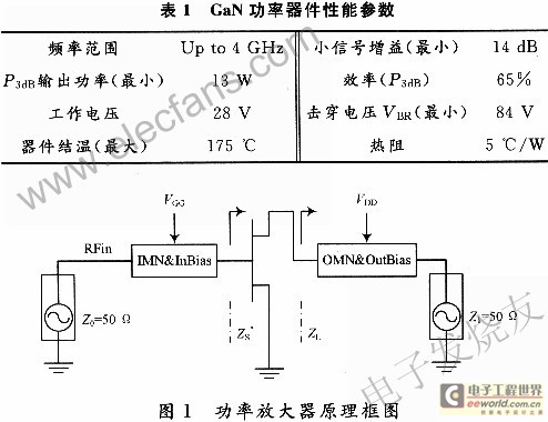
According to the design indicators required by the amplifier, the design uses a SiC-based GaN wide bandgap power tube provided by an imported company. Its main performance parameters are shown in Table 1.
1.3 Amplifier Circuit Design
Figure 1 is a block diagram of the power amplifier. In Figure 1, IMN&Bias and OMN&Bias are the input matching network and input bias circuit and the output matching network and bias circuit, respectively. VGS and VDS are the gate-source operating voltage and drain-source operating voltage, respectively. The design ideas adopted are: conduct DC analysis on the power tube to determine the static operating voltage of the amplifier; conduct stability analysis and design; use the source pull (Source Pull) and load pull (Load Pull) methods to determine the optimal source impedance ZS and optimal load impedance ZL of the power tube matching circuit (see Figure 1 for the definition of ZS and ZL);
According to the obtained source impedance and load impedance, input and output matching circuit design and bias circuit design are carried out; processing, debugging and revision are carried out.
1.3.1 DC Analysis
The purpose of DC analysis of power amplifier is to determine the static working voltage of power tube through the current-voltage (IV) curve of power tube. Since the manufacturer provides the ADS model of power tube, the model is directly used for simulation design in the design (the same below).
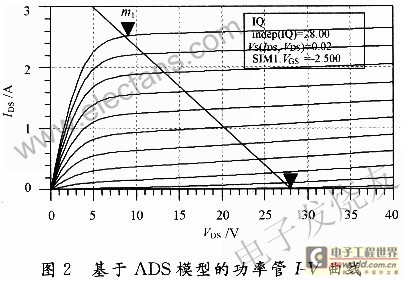
Figure 2 shows the results of DC analysis of the device model in Agilent ADS software. According to the device specifications given by the manufacturer and the IV curve in Figure 2, VDS=28 V and VGS=-2.5 V are selected as the operating voltage of the amplifier. In order to enable the amplifier to achieve higher efficiency, the static voltage is selected here to make the amplifier work under Class C conditions.
1.3.2 Stability Analysis
Stability is one of the key factors to be considered in amplifier design, which depends on the S parameters of the transistor and the terminal conditions. The instability of the power amplifier will produce undesirable parasitic oscillations, resulting in distorted results or even design failure. Therefore, stability analysis and design must be performed before designing the amplifier impedance matching circuit.
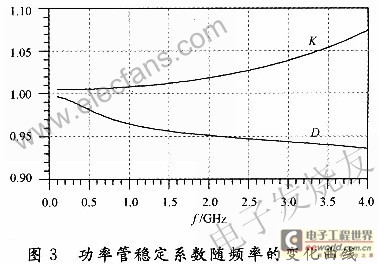
Figure 3 shows the curve of the power tube stability factor changing with frequency. In Figure 3, the stability factors K and D are defined as:

It can be seen from Figure 3 that within the design frequency band, the stability coefficients K and D satisfy the conditions of being greater than 1 and less than 1 respectively, so the power tube is unconditionally stable.
1.3.3 Source-pull and load-pull analysis
Principle of source-pull/load-pull analysis method: When the amplifier is excited by a large signal level, the power tube is analyzed by continuously changing the source impedance/load impedance, and then the equal power curve and equal gain curve are drawn on the Smith impedance circle chart. The optimal source impedance/optimal load impedance is selected according to the design requirements to accurately design a power amplifier that meets the requirements.
The center frequency f=2.35 GHz is selected in the analysis. In order to accurately obtain the optimal source impedance ZS and the optimal output impedance ZL of the power tube, the efficiency-first strategy is followed during the analysis process, and the following steps are taken:
First, assume that ZS(O) = 10 Ω and perform load-pull analysis to obtain ZL(1); then, perform source-pull analysis based on ZL(1) to obtain ZS(1); then perform load-pull analysis based on ZS(1) to obtain ZL(2), ... Repeat the source-pull analysis and load-pull analysis until the load impedances ZL obtained twice are equal or differ very little.
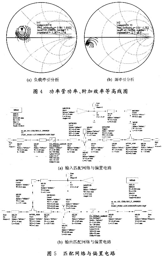
FIG4 is a contour diagram of the power tube output power and power added efficiency (PAE) obtained by performing source pull analysis and load pull analysis. In FIG4, the power tube added efficiency is defined as:
Where: POUT, PIN and PDC are the amplifier output power, input power and power consumption respectively; ηPAE represents the power added efficiency.
From Figure 4, we can see that the optimal source impedance and optimal load impedance of the power amplifier are ZS=2.1-j6.5 Ω and ZL=13+j7.8 Ω respectively.
1.3.4 Matching network and bias circuit design
The matching circuit is mainly used for impedance transformation, and its ultimate goal is to achieve maximum power transmission. In the simulation design process, it is first assumed that the input and output matching network designs are designed using the optimal source impedance and optimal load impedance obtained under the ideal bias circuit, and then the bias circuit is designed according to the 1/4λ criterion, and the bias circuit meets the requirements of the RF choke by fine-tuning some circuit parameters. In Agilent ADS software, in order to make the design accurately simulate the real situation, it is generally necessary to perform RFMomentum optimization simulation after circuit design (model-based). Figure 5 shows the amplifier matching network and bias circuit designed by Agilent ADS software. In Figure 5, the microwave circuit substrate material is Rogers' RT/duroid 6002 board, with a dielectric constant of 2.94 and a thickness of 0.254 mm. During the optimization simulation process, it was found that the efficiency and bandwidth of the amplifier are a contradiction. When the efficiency is improved, the bandwidth becomes narrower, and vice versa.
2. Index test
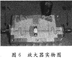
The actual amplifier is shown in Figure 6.
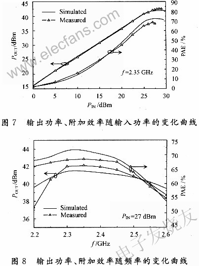
The designed wide bandgap power amplifier was tested. The test conditions are: continuous wave operation, drain voltage VDS=28 V, gate voltage VGS=-2.5 V. Figure 7 shows the curves of the amplifier output power and additional efficiency with input power at a frequency of 2.35 GHz. From the test results, it can be seen that: with the increase of input power, the output power of the amplifier increases approximately linearly, and saturation begins to appear at 26 dBm; with the increase of input power, the amplifier additional efficiency increases, and the maximum additional efficiency reaches 68.5% at 27 dBm. The output power and additional efficiency parameters of the amplifier were also tested in the frequency range of 2.2 to 2.6 GHz (0.5 GHz as a step), and the test results are shown in Figure 8. In the frequency range of 2.25 to 2.5 GHz, the amplifier output power is above 10 W, and the additional efficiency is also over 60%. In the frequency range of 2.3 to 2.4 GHz, the output power exceeds 15 W, the additional efficiency exceeds 67 9/6, and the amplifier meets the design indicators.
3 Conclusion
An S-band 10 W power amplifier was designed and fabricated using SiC-based GaN wide bandgap power devices. The test results show that the designed amplifier has an additional efficiency of more than 67 9/6 in the range of 2.3 to 2.4 GHz, which also confirms the high efficiency and high gain characteristics of wide bandgap devices.
Previous article:Discussion on GPS Clock Generator (GPS Synchronous Clock)
Next article:High-speed arbitrary waveform generator based on digital frequency synthesis technology
Recommended ReadingLatest update time:2024-11-16 19:51


- Popular Resources
- Popular amplifiers
-
 Operational Amplifier Practical Reference Handbook (Edited by Liu Changsheng, Zhao Mingying, Liu Xu, etc.)
 -
 A review of deep learning applications in traffic safety analysis
 -
 A review of learning-based camera and lidar simulation methods for autonomous driving systems
 -
 ARM Embedded System Principles and Applications (Wang Xiaofeng)
- High signal-to-noise ratio MEMS microphone drives artificial intelligence interaction
- Advantages of using a differential-to-single-ended RF amplifier in a transmit signal chain design
- ON Semiconductor CEO Appears at Munich Electronica Show and Launches Treo Platform
- ON Semiconductor Launches Industry-Leading Analog and Mixed-Signal Platform
- Analog Devices ADAQ7767-1 μModule DAQ Solution for Rapid Development of Precision Data Acquisition Systems Now Available at Mouser
- Domestic high-precision, high-speed ADC chips are on the rise
- Microcontrollers that combine Hi-Fi, intelligence and USB multi-channel features – ushering in a new era of digital audio
- Using capacitive PGA, Naxin Micro launches high-precision multi-channel 24/16-bit Δ-Σ ADC
- Fully Differential Amplifier Provides High Voltage, Low Noise Signals for Precision Data Acquisition Signal Chain
- Innolux's intelligent steer-by-wire solution makes cars smarter and safer
- 8051 MCU - Parity Check
- How to efficiently balance the sensitivity of tactile sensing interfaces
- What should I do if the servo motor shakes? What causes the servo motor to shake quickly?
- 【Brushless Motor】Analysis of three-phase BLDC motor and sharing of two popular development boards
- Midea Industrial Technology's subsidiaries Clou Electronics and Hekang New Energy jointly appeared at the Munich Battery Energy Storage Exhibition and Solar Energy Exhibition
- Guoxin Sichen | Application of ferroelectric memory PB85RS2MC in power battery management, with a capacity of 2M
- Analysis of common faults of frequency converter
- In a head-on competition with Qualcomm, what kind of cockpit products has Intel come up with?
- Dalian Rongke's all-vanadium liquid flow battery energy storage equipment industrialization project has entered the sprint stage before production
- Allegro MicroSystems Introduces Advanced Magnetic and Inductive Position Sensing Solutions at Electronica 2024
- Car key in the left hand, liveness detection radar in the right hand, UWB is imperative for cars!
- After a decade of rapid development, domestic CIS has entered the market
- Aegis Dagger Battery + Thor EM-i Super Hybrid, Geely New Energy has thrown out two "king bombs"
- A brief discussion on functional safety - fault, error, and failure
- In the smart car 2.0 cycle, these core industry chains are facing major opportunities!
- The United States and Japan are developing new batteries. CATL faces challenges? How should China's new energy battery industry respond?
- Murata launches high-precision 6-axis inertial sensor for automobiles
- Ford patents pre-charge alarm to help save costs and respond to emergencies
- New real-time microcontroller system from Texas Instruments enables smarter processing in automotive and industrial applications
- Creative PCB display
- LPC2478 Timer 2 and Timer 3 enable
- Design and implementation of optical transceiver UART interface based on FPGA.pdf
- MicroPython official new wiki
- Is this setting OK?
- Daisy chain communication
- EEWORLD University Hall ---- Sharing of infusion pump application reference solutions based on Lingdong MM32F series large-capacity MCU
- TI C5000 Ultra-Low-Power DSP
- Instrument Oscilloscope Tutorial Video Live Replay Summary (Continuously Updated)
- [Personal Test] Notes on "jumping pits" in diode voltage test - onboard test verification of hardware

 Operational Amplifier Practical Reference Handbook (Edited by Liu Changsheng, Zhao Mingying, Liu Xu, etc.)


 京公网安备 11010802033920号