An asynchronous counter circuit refers to a circuit whose basic functional unit trigger has a clock input signal that is not together with the trigger. Some are external input pulse signals, and some are outputs of other triggers. This article gives a design scheme for an N-ary asynchronous counter .
1. How to select the clock signal for each trigger
The change of the trigger state must be triggered by a trigger pulse. Therefore, when selecting the clock signal for each trigger, it must be satisfied that the trigger signal arrives at the moment when all the states of the trigger change. At the same time, the number of trigger signals arriving for the unchanged state should be as small as possible. According to the second principle, referring to the design of the binary asynchronous counter, the selection of the clock signal of each trigger starts from the previous one. For example, when selecting the CP3 signal of the Q3 trigger, first check whether the output of Q2 meets the first principle mentioned above. If not, then check the output of Ql, and continue forward until a clock signal that meets the requirements is selected.
2. How to design the simplest form of activation function
Since the selected CP signal corresponds to an unchanged state without the arrival of a pulse, no matter what the input value of the trigger is, the trigger state without a pulse will not change. When designing, this state is regarded as an "irrelevant item", which can make the designed excitation function simpler.
Let's take an 11-base counter as an example. Designing an 11-base counter requires at least 4 triggers, whose states correspond to Q3 Q2 Q1 Q0. The attached table is a simplified state table of the 11-base counter. Two adjacent rows: the previous row is the "current state" of the next row, and the next row is the "next state" of the previous row. According to the attached table, it is relatively easy to complete the first step of the design: select the CP pulse for each trigger (assuming the trigger is a falling edge trigger).
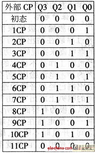
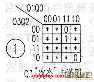
Design of Q3 trigger clock signal CP3: First observe Q2, and find that when the Q3 state changes from "0" to "1", Q2 has a downward jump pulse, but when Q3 changes from "1" to "0", Q2 does not change, so Q2 cannot be used as the clock signal of Q3 trigger; observe the two changes of Q1 and Q3, Q1 has a downward jump pulse, so CP3=Q1.
Design of Q2 trigger clock signal CP2: First observe the two state changes of Ql and Q2 (when the external 4CP is, Q2 changes from "0" to "1"; when 8CP is, Q2 changes from "1" to "0"), both correspond to Q1 having a down-jump trigger, so CP2=Q1.
Design of the clock signal CP1 of the Q1 trigger: When 11CP comes from the outside, Q1 changes from "1" to "0", but Q0 has no corresponding down-jump pulse, so only the external clock signal can be selected as CPI, that is, CP1=CP. CP0=CP of the Q0 trigger.
If the selected trigger is rising edge triggered, just select the Q of the corresponding trigger as the CP signal.
After selecting the clock signal of each trigger, start designing the trigger's excitation function: according to the attached table and the CP pulse signal of the trigger, draw the "next state" Karnaugh map of each trigger, obtain the "next state" equation, and then obtain the excitation function according to the type of selected trigger.
Q3's "next state" equation: As can be seen from the attached table, Q1 has three down-jump triggers as CP3. When the "current states" are 0011, 0111, and 1010, the corresponding "next states" of Q3 are "0", "1", and "0" respectively, and are filled in Figure 1. Since there is no CP pulse trigger in other states, no matter "0" or "1" is filled in the Karnaugh map in Figure 1, the state remains unchanged and can be regarded as "irrelevant terms" to obtain the simplest "next state" equation. In addition, 1011-1111 are real "irrelevant terms". According to Figure 1, Q3n+1=Q2.
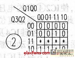
If CP3=CP is selected, a trigger pulse will arrive in each state, so the "next state" Karnaugh map is shown in Figure 2, and the resulting equation is more complicated.
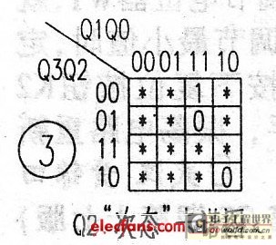
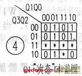
The "sub-state" equation of Q1: CPI=CP, each state has the arrival of a trigger pulse, and the "sub-state" Karnaugh map is shown in Figure 4, Qln+1=Q0Q1+Q3Q0Q1.
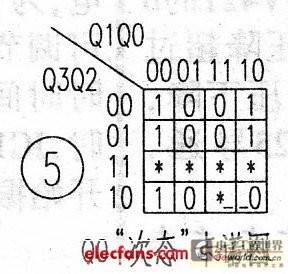
The "sub-state" equation of Q0 is: CP0=CP, and the "sub-state" Karnaugh map is shown in Figure 5, Q0n+1=QlQ0+Q3Q0.
If a JK flip-flop is used, the above "next state" equations are compared with the characteristic equation of the JK flip-flop Qn+1=JQ+KQ, and the driving functions of each flip-flop are obtained: J3=Q2, K3=Q2; J2=Q3, K2=1; J1=Q0, K1=Q3 Q0; JO=Q3 Q1, KO=1.
Finally, the circuit was found to have self-starting capability. Draw the logic circuit, see Figure 6.

Previous article:Low Noise Fractional-N Phase-Locked Loop Implementation
Next article:Application case of infrared thermometer based on EFM32
- High signal-to-noise ratio MEMS microphone drives artificial intelligence interaction
- Advantages of using a differential-to-single-ended RF amplifier in a transmit signal chain design
- ON Semiconductor CEO Appears at Munich Electronica Show and Launches Treo Platform
- ON Semiconductor Launches Industry-Leading Analog and Mixed-Signal Platform
- Analog Devices ADAQ7767-1 μModule DAQ Solution for Rapid Development of Precision Data Acquisition Systems Now Available at Mouser
- Domestic high-precision, high-speed ADC chips are on the rise
- Microcontrollers that combine Hi-Fi, intelligence and USB multi-channel features – ushering in a new era of digital audio
- Using capacitive PGA, Naxin Micro launches high-precision multi-channel 24/16-bit Δ-Σ ADC
- Fully Differential Amplifier Provides High Voltage, Low Noise Signals for Precision Data Acquisition Signal Chain
- Innolux's intelligent steer-by-wire solution makes cars smarter and safer
- 8051 MCU - Parity Check
- How to efficiently balance the sensitivity of tactile sensing interfaces
- What should I do if the servo motor shakes? What causes the servo motor to shake quickly?
- 【Brushless Motor】Analysis of three-phase BLDC motor and sharing of two popular development boards
- Midea Industrial Technology's subsidiaries Clou Electronics and Hekang New Energy jointly appeared at the Munich Battery Energy Storage Exhibition and Solar Energy Exhibition
- Guoxin Sichen | Application of ferroelectric memory PB85RS2MC in power battery management, with a capacity of 2M
- Analysis of common faults of frequency converter
- In a head-on competition with Qualcomm, what kind of cockpit products has Intel come up with?
- Dalian Rongke's all-vanadium liquid flow battery energy storage equipment industrialization project has entered the sprint stage before production
- Allegro MicroSystems Introduces Advanced Magnetic and Inductive Position Sensing Solutions at Electronica 2024
- Car key in the left hand, liveness detection radar in the right hand, UWB is imperative for cars!
- After a decade of rapid development, domestic CIS has entered the market
- Aegis Dagger Battery + Thor EM-i Super Hybrid, Geely New Energy has thrown out two "king bombs"
- A brief discussion on functional safety - fault, error, and failure
- In the smart car 2.0 cycle, these core industry chains are facing major opportunities!
- The United States and Japan are developing new batteries. CATL faces challenges? How should China's new energy battery industry respond?
- Murata launches high-precision 6-axis inertial sensor for automobiles
- Ford patents pre-charge alarm to help save costs and respond to emergencies
- New real-time microcontroller system from Texas Instruments enables smarter processing in automotive and industrial applications
- 【Me and Yatli】+My impression of Yatli
- Advanced Algebra Concise Course
- AP6212 driver all firmware & nvram
- Bosch air pressure sensor gives sweeping robots more monitoring functions
- 8 output modes of MSP430 microcontroller
- FPGA learning notes-----Fixing the program through JTAG
- More than just GaN! Qorvo's three key advantages in leading 5G era technologies
- PCB 3D component library
- Award-winning live broadcast | Beneng International launches millimeter-wave radar module based on Infineon technology, perfectly solving the pain points of the PIR market. Registration is open
- The principle of BLDC square wave sensorless control based on ADC sampling and integration

 【ON Semiconductor】LC87F7932B8-bit single-chip microcontroller
 IEEE 1394 FireWire protocol standard


 京公网安备 11010802033920号