As shown in the figure, this is a type of single-chip AD converter:
ADC0804 is a monolithic integrated A/D converter. It uses a 20-pin integrated chip with CMOS technology, a resolution of 8 bits, a conversion time of 100µs, and an input voltage range of 0 to 5V. The chip has a three-state output data latch that can be directly connected to the data bus.
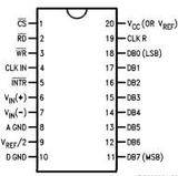
The names and functions of each pin are as follows:
VIN(+), VIN(-) - two analog signal input terminals, used to receive unipolar, bipolar and differential input signals.
DB7~DB0——Digital signal output port with three-state characteristics.
AGND——Analog signal ground.
DGND——digital signal ground.
CLK——Clock signal input terminal.
CLKR - The external resistor end of the internal clock generator, which cooperates with the CLK end to generate clock pulses by the chip itself, and its frequency is 1/(1.1RC).
CS#---Chip select signal input terminal, low level is valid. Once CS# is valid, it indicates that the A/D converter is selected and can start working.
WR#---Write signal input, low level starts A/D conversion.
RD#---Read signal input, low level output terminal is valid.
INTR#---A/D conversion end signal, low level is valid to indicate that the conversion is completed.
VREF/2---Reference level input, determines the quantization unit.
VCC---Chip power 5V input.
Opening the data sheet of ADC0804, we can see the following typical circuit connection:
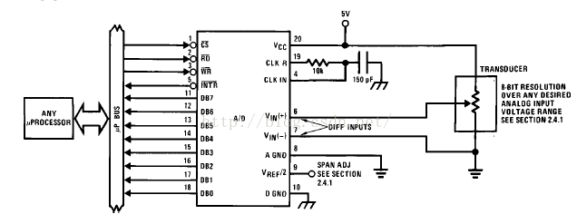
We can draw it using simulation software:
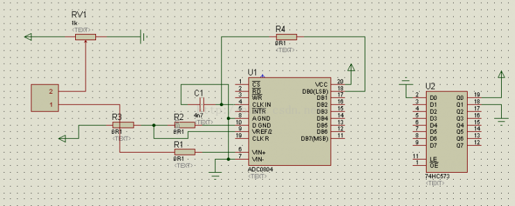
Next, let's analyze how the above figure works:
①The chip select terminal CS of ADC0804 is connected to the Q7 output terminal of U2 latch. We can control CS by controlling the latch. The reason for this connection is that the TX-1C experimental board has too many peripheral expansions and there are no extra I/O ports to independently control the CS terminal of ADC0804, so U2 is selected.
② VIN(+) is connected to the middle sliding end of the potentiometer, and VIN(-) is grounded, because these two ends can input differential voltage, that is, it can measure the voltage between VIN(+) and VIN(-). When VIN(-) is grounded, the voltage at the VIN(+) end is the analog input voltage of ADC0804. A 10kΩ resistor is connected in series between VIN(+) and the potentiometer to limit the current flowing into the VIN(+) end to prevent the A/D chip from being burned out due to excessive current. When the ADIN pin is shorted with a shorting cap, the middle sliding end of the potentiometer is connected to VIN(+) through resistor R12. At this time, when the potentiometer knob is adjusted, the voltage at the middle sliding end changes from 0 to VCC, and then the digital output end of ADC0804 also changes from 0x00 to 0xFF.
③ The resistor and capacitor form an RC oscillator circuit between CLKR, CLR and GND to provide the pulses required for the ADC0804 to work. The frequency of the pulse is 1/(1.1RC). According to the chip manual, R is 10kΩ and C is 150pF. In order to reduce the number of components and facilitate welding on the TX-1C experimental board, C uses a 104 magnetic chip capacitor. When designing your own circuit, you can choose a 150pF capacitor, otherwise it will affect the A/D conversion rate.
④ Use two 1kΩ resistors to divide the VREF/2 terminal to get the VCC/2 voltage, that is, 2.5V, which is used as the internal reference voltage when the A/D chip is working.
⑤WR# and RD# are connected to the P3.6 and P3.7 pins of the microcontroller respectively, and the digital output terminal is connected to the P1 port of the microcontroller.
⑥ Connect AGND and DGND to the GND of the experimental board at the same time. When we design products, if we use A/D and D/A, these chips generally provide independent analog ground (AGND) and digital ground (DGND) pins. In order to achieve high accuracy and good stability, it is best to connect the analog ground and digital ground of all devices separately, and finally connect the analog ground and digital ground at only one point.
⑦ INTR# pin is not connected. The interrupt method is not used to read A/D data on the TX-1C experimental board, so this pin can be disconnected. When operating a digital chip, its operation timing diagram must be analyzed first. Figure 4.4.6 is the start conversion timing diagram of ADC0804.
ADC0804 conversion timing diagram:
From the analysis of Figure 4.4.6, we can see that CS is low first, and then WR# is set low. After at least tW(WR#)L time, WR# is pulled high, and then the A/D converter is started. After (1 to 8 A/D clock cycles + internal TC) time, the analog/digital conversion is completed, and the conversion result is stored in the data latch. At the same time, INTR automatically becomes low, notifying the microcontroller that the conversion has ended. The size of the several times is explained in the chip manual.
When I write a microcontroller program to start A/D conversion, I have to follow the above timing. Since the TX-1C experimental board does not use interrupts to read A/D data, we wait for a while after starting A/D conversion, and then directly read the A/D digital output port. After reading, start an A/D conversion, and so on. Figure 4.4.7 is the timing diagram of ADC0804 reading data.
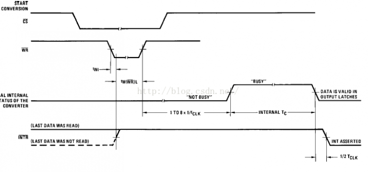
From the above figure, we can see that CS is low first, then WR# is set low, and after at least tW(WR#)L time, WR# is pulled high, and then the A/D converter is started, and after (1 to 8 A/D clock cycles + internal TC) time, the analog/digital conversion is completed, and the conversion result is stored in the data latch. At the same time, INTR automatically becomes low, notifying the microcontroller that the conversion has ended. The size of the several times is explained in the chip manual.
When I write a microcontroller program to start A/D conversion, I have to follow the above timing. Since the TX-1C experimental board does not use interrupts to read A/D data, we wait for a while after starting the A/D conversion, and then directly read the A/D digital output port. After reading, start an A/D conversion, and so on. The figure below is the timing diagram of ADC0804 reading data.
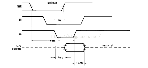
From the above figure, we can see that when INTR# becomes a low level, CS# is set low first. After RD# is set low for at least tACC time, the data on the digital output port reaches a stable state. At this time, the digital signal can be obtained by directly reading the data on the digital output port. After reading the data, RD# is immediately pulled high, and then CS# is pulled high. INTR# changes automatically. When RD# is set low for tR1 time, INTR# is automatically pulled high, and we do not need to intervene manually.
Figure 4.4.6 and Figure 4.4.7 are the timing diagrams of ADC0804 starting conversion and reading data. This is the timing diagram of starting once and reading data once. When we want to convert continuously and read data continuously, is it necessary to set CS# low and then high every time? Because CS# is the chip select signal, setting it low means that the chip can be operated or is in a normal working state. So when writing the program, just set CS# low at the beginning, and then when you want to start the conversion and read the data, you only need to operate WR# and RD#.
Previous article:51 MCU stack
Next article:The process of microcontroller executing program, deepen the understanding of 51 microcontroller instructions
Recommended ReadingLatest update time:2024-11-24 11:30


- Popular Resources
- Popular amplifiers
-
 Microgrid Stability Analysis and Control Microgrid Modeling Stability Analysis and Control to Improve Power Distribution and Power Flow Control (
 -
 Wireless Sensor Network Technology and Applications (Edited by Mou Si, Yin Hong, and Su Xing)
 -
 Modern Electronic Technology Training Course (Edited by Yao Youfeng)
 -
 Modern arc welding power supply and its control
- Naxin Micro and Xinxian jointly launched the NS800RT series of real-time control MCUs
- How to learn embedded systems based on ARM platform
- Summary of jffs2_scan_eraseblock issues
- Application of SPCOMM Control in Serial Communication of Delphi7.0
- Using TComm component to realize serial communication in Delphi environment
- Bar chart code for embedded development practices
- Embedded Development Learning (10)
- Embedded Development Learning (8)
- Embedded Development Learning (6)
 Professor at Beihang University, dedicated to promoting microcontrollers and embedded systems for over 20 years.
- Intel promotes AI with multi-dimensional efforts in technology, application, and ecology
- ChinaJoy Qualcomm Snapdragon Theme Pavilion takes you to experience the new changes in digital entertainment in the 5G era
- Infineon's latest generation IGBT technology platform enables precise control of speed and position
- Two test methods for LED lighting life
- Don't Let Lightning Induced Surges Scare You
- Application of brushless motor controller ML4425/4426
- Easy identification of LED power supply quality
- World's first integrated photovoltaic solar system completed in Israel
- Sliding window mean filter for avr microcontroller AD conversion
- What does call mean in the detailed explanation of ABB robot programming instructions?
- STMicroelectronics discloses its 2027-2028 financial model and path to achieve its 2030 goals
- 2024 China Automotive Charging and Battery Swapping Ecosystem Conference held in Taiyuan
- State-owned enterprises team up to invest in solid-state battery giant
- The evolution of electronic and electrical architecture is accelerating
- The first! National Automotive Chip Quality Inspection Center established
- BYD releases self-developed automotive chip using 4nm process, with a running score of up to 1.15 million
- GEODNET launches GEO-PULSE, a car GPS navigation device
- Should Chinese car companies develop their own high-computing chips?
- Infineon and Siemens combine embedded automotive software platform with microcontrollers to provide the necessary functions for next-generation SDVs
- Continental launches invisible biometric sensor display to monitor passengers' vital signs
- Inductor and transformer testing methods and experience
- Help!!! Course Design - Detection of DC Motor Working Current
- Asynchronous IO principles and corresponding functions
- ARM11 processor performance exceeds 750MHz
- What is NFC, a wireless communication technology, and what impact does it have on our lives?
- What embedded operating system are you using?
- 【ufun learning】Analysis of the buzzing routine
- MSP430F413 Fruit Battery Powered Low Power Clock
- I want to transfer the Verilog module compiled by Quartus II 5.0 to Multisim 2001 for system simulation.
- [Evaluation and experience of Zhongke Yihaiwei EQ6HL45 development platform] +02.eLinx software installation (zmj)

 Microgrid Stability Analysis and Control Microgrid Modeling Stability Analysis and Control to Improve Power Distribution and Power Flow Control (


 京公网安备 11010802033920号