Functional realization goal
The PWM output IO multiplexing of the CH3 channel of TIM2 can be realized by writing the option byte, and can be set to PA3 or PD2 output.
Option Byte
The option bytes include the configuration of the chip hardware features and the protection information of the memory. These bytes are stored in a dedicated block in the memory. In addition to the ROP (read-out protection) byte, each option byte must be saved twice, one in the usual format (OPTx) and one in the backup complementary format (NOPTx). The option bytes can be modified by the application in IAP mode, but the ROP option can only be modified in ICP mode (through SWIM). For the content of the SWIM programming process, please refer to the STM8S Flash Programming Manual (PM0051) and the STM8 SWIM Communication Protocol and Debug Module User Manual (UM0470).
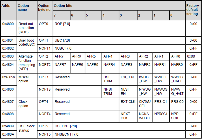
The option bytes of different chips are different in size. For details, please refer to the chip data sheet. Taking STM8S103F3 as an example, the option bytes are as follows:
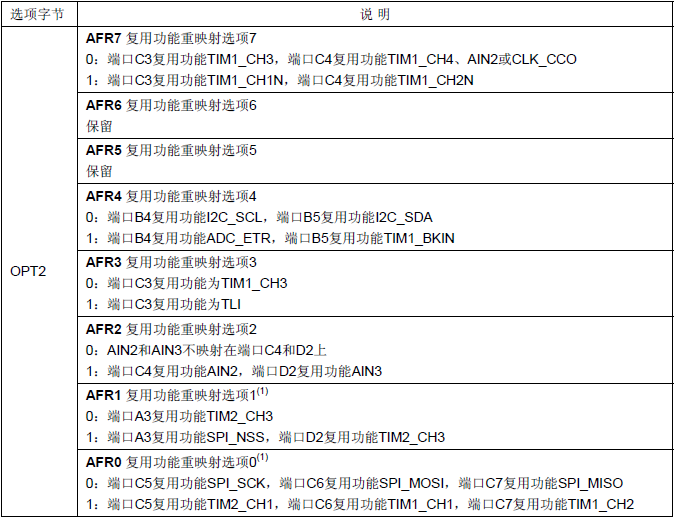
STM8S103F redefines the multiplexing function bits for 20-pin package products:
From this we can know that we need to write the AFR1 bit in the OPT2 byte. By writing 0, port A3 multiplexes the function TIM2_CH3, and by writing 1, port D2 multiplexes the function TIM2_CH3. Next, implement this function through the program. You can modify the value of AFR1 to see if the PWM output switches the pin. If it can, the write operation is implemented.
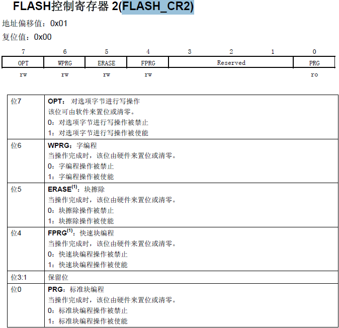
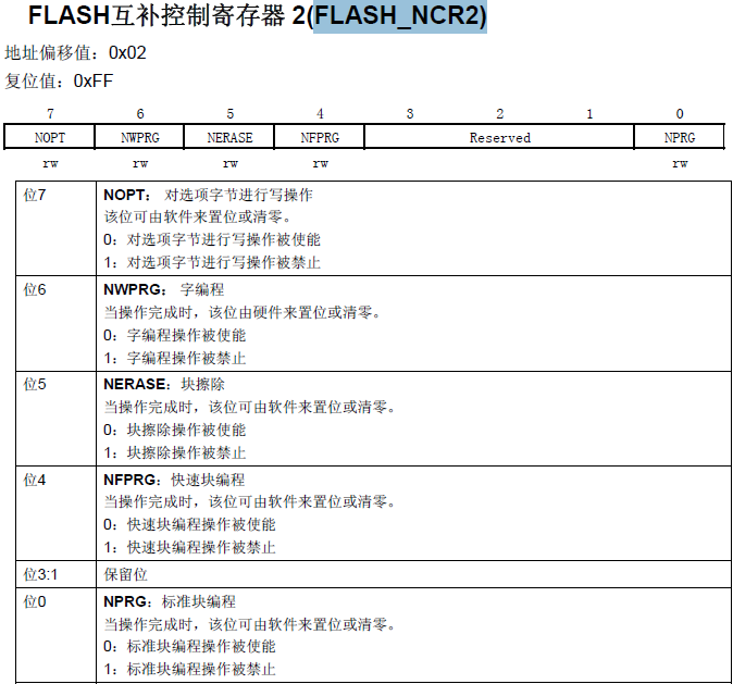
The option bytes are stored in the EEPROM, so the option bytes can be modified in the same way as reading and writing EEPROM. The application can write directly to the target address. We already know the address from the figure above: 0x4803, 0x4804. The configuration of the register can be found in the reference manual (RM0016).
Related register operations:
Test program implementation
Note: When implementing the program to erase Option Bytes, the application cannot be run, otherwise an error will occur! But I still think this is a bit troublesome. It would be better to use STVP to erase and write. It would be great if it can be put in the application to erase and write. Is it so troublesome to use the program to implement multiplexing? I hope to explore and find a good method. In the end, I only found an unreliable one, which is to add a delay after erasing, but this sometimes works and sometimes doesn't. Or should I check the information to see what's going on?
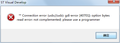
But when using STVP to erase, I encountered this error:
Error : Error on Option Bytes (complementary bytes). Reprogram Option Bytes of device
Error: < OPTION BYTE verifying failed.123
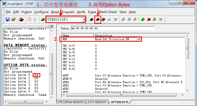
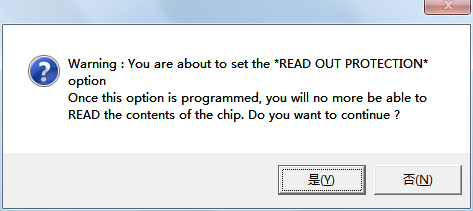
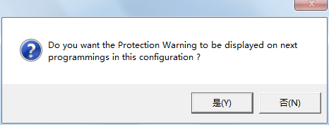
Use STVP to erase Option Bytes. First set ROP to ON, then erase Option Bytes. Two prompt boxes will appear. Select Yes (Y). Then set ROP to OFF again and erase Option Bytes again. Then you can use STVD to burn the program and simulate through stlink.
test program:
/* MAIN.C file
Functons: Operate the option byte, set IO multiplexing, and modify the PWM output pin PA3 or PD2 of CH3 channel of TIM2
Date : July 22, 2015
Author : yicm
Notes:
*/
#include
void CLK_init(void)
{
CLK_ICKR |= 0X01; //Enable internal high-speed clock HSI
CLK_CKDIVR = 0x08; //16M internal RC is divided by 2 and the system clock is 8M
while(!(CLK_ICKR&0x02)); //HSI is ready
CLK_SWR=0xe1; //HSI is the main clock source
}
void Init_GPIO(void)
{
/*Set to push-pull output, PD2 is connected to LED light*/
PD_DDR |= 0X04; //Set PD2 port to output mode
PD_CR1 |= 0X04; //Set PD2 port to push-pull output mode
PD_CR2 &= 0XFD;
PA_DDR |= 0X08; //Set PA3 port to output mode
PA_CR1 |= 0X08; //Set PA3 port to push-pull output mode
PA_CR2 |= 0XF7;
}
void Init_Tim2(void)
{
TIM2_CCMR3 |= 0X70; //Set the output comparison mode of timer 2 three channels (PD2)
TIM2_CCMR3 |= 0X04; //Output compare 3 preload enable
TIM2_CCER2 |= 0x03; //Channel 3 is enabled, low level is valid, and it is configured as output
// Initialize the clock divider to 1, that is, the clock frequency of the counter is Fmaster=8M/64=0.125MHZ
TIM2_PSCR = 0X07;
// Initialize the auto-load register to determine the frequency of the PWM square wave, Fpwm=0.125M/62500=2HZ
TIM2_ARRH = 62500/256;
TIM2_ARRL = 62500%256;
// Initialize the comparison register to determine the duty cycle of the PWM square wave: 5000/10000 = 50%
TIM2_CCR3H = 31250/256;
TIM2_CCR3L = 31250%256;
//Start counting; Update interrupt disable
TIM2_CR1 |= 0x81;
//TIM2_IER |= 0x00;
}
void Write_Option_Byte(void)
{
unsigned char opt[6] = {0,0,0x00,0,0,0};
/*Unlock Flash*/
do
{
FLASH_DUKR = 0xAE;
FLASH_DUKR = 0x56;
}
while(!(FLASH_IAPSR & 0X08));
/*Enable write operation to option bytes*/
FLASH_CR2 = 0X80;
/*Complementary control register*/
FLASH_NCR2 = 0X7F;
/*Write operation, 0x02: PD2. 0x00: PA3*/
*((unsigned char *)0x4800) = opt[0];
*((unsigned char *)0x4801) = opt[1];
*((unsigned char *)0x4802) = ~opt[1];
*((unsigned char *)0x4803) = opt[2];
*((unsigned char *)0x4804) = ~opt[2];
*((unsigned char *)0x4805) = opt[3];
*((unsigned char *)0x4806) = ~opt[3];
*((unsigned char *)0x4807) = opt[4];
*((unsigned char *)0x4808) = ~opt[0];
*((unsigned char *)0x4809) = opt[5];
*((unsigned char *)0x480A) = ~opt[5];
/*Wait for writing to complete*/
while(!(FLASH_IAPSR & 0x04));
}
main()
{
int i;
Write_Option_Byte(); //When running the program, shield
for(i=0;i<10000;++i); //Delay effect. Sometimes adding a delay can make the erase and application program work without blocking at the same time.
CLK_init(); //Shield during erase, otherwise an error will occur during the next stlink simulation
Init_GPIO(); //Shield during erase, otherwise an error will occur during the next stlink simulation
Init_Tim2(); //Shield during erase, otherwise an error will occur during the next stlink simulation
while (1);
}
Previous article:The difference between PLC control and single chip microcomputer control
Next article:STM8S---Power consumption management halt mode (halt) implementation
Recommended ReadingLatest update time:2024-11-16 03:52


- Popular Resources
- Popular amplifiers
 Professor at Beihang University, dedicated to promoting microcontrollers and embedded systems for over 20 years.
- LED chemical incompatibility test to see which chemicals LEDs can be used with
- Application of ARM9 hardware coprocessor on WinCE embedded motherboard
- What are the key points for selecting rotor flowmeter?
- LM317 high power charger circuit
- A brief analysis of Embest's application and development of embedded medical devices
- Single-phase RC protection circuit
- stm32 PVD programmable voltage monitor
- Introduction and measurement of edge trigger and level trigger of 51 single chip microcomputer
- Improved design of Linux system software shell protection technology
- What to do if the ABB robot protection device stops
- Allegro MicroSystems Introduces Advanced Magnetic and Inductive Position Sensing Solutions at Electronica 2024
- Car key in the left hand, liveness detection radar in the right hand, UWB is imperative for cars!
- After a decade of rapid development, domestic CIS has entered the market
- Aegis Dagger Battery + Thor EM-i Super Hybrid, Geely New Energy has thrown out two "king bombs"
- A brief discussion on functional safety - fault, error, and failure
- In the smart car 2.0 cycle, these core industry chains are facing major opportunities!
- The United States and Japan are developing new batteries. CATL faces challenges? How should China's new energy battery industry respond?
- Murata launches high-precision 6-axis inertial sensor for automobiles
- Ford patents pre-charge alarm to help save costs and respond to emergencies
- New real-time microcontroller system from Texas Instruments enables smarter processing in automotive and industrial applications
- EEWORLD University Hall----TI motor driver chip latest technical advantages and applications
- 【ufun learning】Learning chapter 6: "Basic routine 5 - touch button control-PWM"
- 【Development and application based on NUCLEO-F746ZG motor】16. Function calculation of safety tasks - temperature calculation
- [Sipeed LicheeRV 86 Panel Review] 1- Unboxing Review
- EEWORLD University ---- Live Replay: How to complete efficient and reliable USB PD power design in minutes - PI Expert? Step-by-step tutorial
- TI Embedded Processors Live Review Highlights (2020)
- 【Repost】 Thirty Practical Experiences in Switching Power Supply Design (Part 2)
- Tin storage rosin splash
- I feel like I won't receive my NXP IoT until next year.
- threadx is now open source

 ARM Cortex M4 cookbook


 京公网安备 11010802033920号