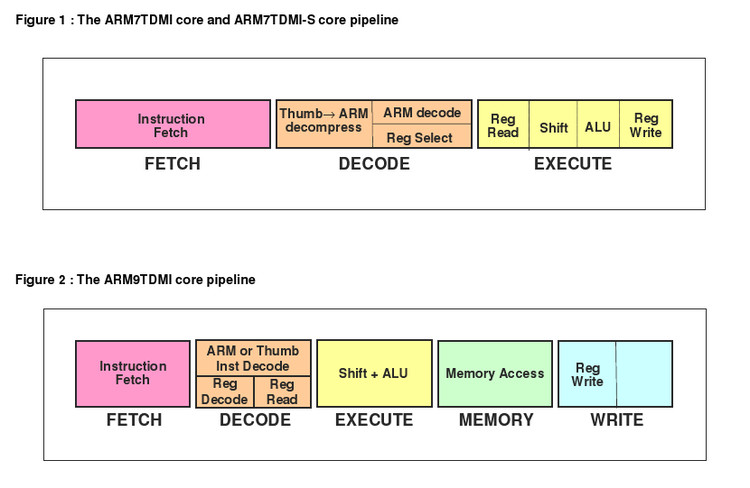
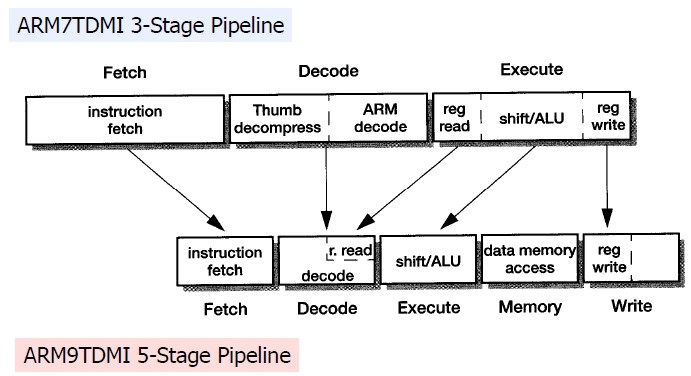
ARM7 uses a three-stage pipeline
(1) Fetch:
The task of the fetch stage is to read instructions from the program memory.
(2) Decode:
The decode stage completes the analysis of the instruction and prepares the control signals required by the data path for the next cycle. At this stage, the instruction occupies the decoding logic and does not occupy the data path.
(3) Execute:
Complete the operation required by the instruction and write the result back to the register as needed. The instruction occupies the data path, the register stack is read, and the operand is shifted in the barrel row shifter. The operator generates the operation result and writes it back to the destination register. The operator changes the conditional bit of the status register according to the instruction requirements and the transport result.
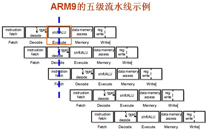
ARM9 uses a five-stage pipeline
(1) fetch
Instructions are fetched from memory and placed into the instruction pipeline.
(2) Decode
The instruction is decoded and the register operands are read from the register file. There are three operand read ports in the register file, so most ARM instructions can read their operands in 1 cycle.
(3) Execute
One of the operands is shifted and the result is produced in the ALU. If the instruction is a load or store instruction, the address of the memory is calculated in the ALU.
(4) Buffer/data
If necessary, the data memory is accessed, otherwise the ALU is simply buffered for one clock cycle so that all instructions have the same pipeline flow.
(5) Write-back register stack
--------------------------------------------------------
Note that in arm7, execution and instruction fetch are separated by a decoding level, which does not read data, and the current PC = original PC + 8.
In normal arm9, the decoding level between execution and instruction fetch is no longer honest, and the decoding level has begun to read register operands from the register stack. In this case,
what is read is PC + 4, not PC + 8, and the execution level will not read it again, which will cause the PC of the execution level to still = PC + 4.
In order to maintain backward compatibility, on the ARM9's 5-level pipeline, the PC value added by the instruction fetch level is directly sent to the register of the decoding level, passing through the pipeline register between the two levels, so that the PC value obtained by the decoding level is the PC + 4 of the next instruction, which is equal to the PC + 8 of the current instruction.
When it reaches the execution level, the value of the PC register = the current instruction address + 8
When using the STR or STM instruction to save R15, the current instruction address plus 8 or the current instruction address plus 12 may be saved.
Which method is used depends on the specific design of the chip. Of course, only one method can be used in the same chip. Either save the current instruction address plus 8 or save the current instruction address plus 12. Program developers should try to avoid using the STR or STM instruction to operate R15. When this method is unavoidable, you can first use a small program to determine which method the chip used is implemented. For example:
SUB R1,PC, #4; Store the STR instruction address in
R1STR PC,[R0]; Use the STR instruction to save PC to the address unit pointed to by R0,;
PC = STR instruction address + offset (offset is 8 or 12).
LDR R0,[R0]; Read the value of STR instruction address + offsetSUB
R0,R0,R1; Subtract the address of the STR instruction from the value of the STR instruction address + offset,;
Get the offset value (8 or 12).
=============================
ARM7 uses a three-stage pipeline von Neumann structure, and ARM9 uses a five-stage pipeline Harvard structure.
The ARM7 pipeline includes fetch, decode, and execute. The ARM7 pipeline does not read the operand register in the decode stage, so the relationship between the PC value in the execute stage and the PC value in the fetch stage is: PC (execute) = PC (fetch) + 8.
The ARM9 pipeline includes fetch, decode, execute, buffer/data, and write-back register stacks. The ARM9 pipeline has already started reading operand registers in the decode stage, so the relationship between the PC value in the decode stage and the PC value in the fetch stage is: PC(decode)=PC(fetch)+4. Therefore, the relationship between the PC value in the execute stage and the PC value in the decode stage is: PC(execute)=PC(decode)+4.
In order to ensure the compatibility of the ARM9 pipeline and the ARM7 pipeline, the ARM9 pipeline sends the PC value of the instruction fetch stage directly to the decode stage register, bypassing the instruction fetch and decode pipeline registers. This still ensures that the relationship between the PC value of the execution stage and the PC value of the instruction fetch stage is: PC (execute) = PC (fetch) + 8.


Take the following assembly code of start.S in uboot as an example to explain:
00000000 <_start>:
0: ea000014 b 58
4: e59ff014 ldr pc, [pc, #20] ; 20 <_undefined_instruction>
8: e59ff014 ldr pc, [pc, #20] ; 24 <_software_interrupt>
c: e59ff014 ldr pc, [pc, #20] ; 28 <_prefetch_abort>
10: e59ff014 ldr pc, [pc, #20] ; 2c <_data_abort>
14: e59ff014 ldr pc, [pc, #20] ; 30 <_not_used>
18: e59ff014 ldr pc, [pc, #20] ; 34 <_irq>
1c: e59ff014 ldr pc, [pc, #20] ; 38 <_fiq>
00000020 <_undefined_instruction>:
20: 00000120 .word 0x00000120
Copy code
The following is a detailed description of what the CPU does in each instruction cycle:
Before looking at the specific explanation below, there is one sentence to keep in mind, that is:
The PC does not point to the instruction you are running;
The PC always points to the address of the instruction you want to fetch.
Once you have a clear understanding of this premise, the examples that follow will be easy to understand.
Instruction cycle Cycle1
(1) Instruction fetch:
PC always points to the address of the instruction to be read (that is, we often say, the address of the next instruction), and the current PC = 4,
So the physical address is 4 pairs of instructions corresponding to "ldr pc, [pc, #20]", and its corresponding binary code is e59ff014.
After the instruction is fetched here, the value of PC is automatically updated, that is, PC = PC + 4 (a single instruction occupies 4 bytes, so add 4) = 4 + 4 = 8
Instruction cycle Cycle2
(1) Translation instruction: translation instruction e59ff014;
(2) At the same time, fetch the instruction:
PC always points to the address of the instruction to be read (that is, we often say, the address of the next instruction), and the current PC = 8,
So the instruction corresponding to the physical address 8 is "ldr pc, [pc, #20]", and its corresponding binary code is e59ff014.
After the instruction is fetched here, the value of PC is automatically updated, that is, PC=PC+4=8+4=12=0xc
Instruction cycle Cycle3
(1) Execute (instruction): Execute "e59ff014", which means "ldr pc,[pc, #20]", that is,
PC
= PC + 20
= 12 + 20
= 32
= 0x20
Here, we just calculate that the value to be assigned to PC is 0x20, and this 0x20 is just placed in the internal buffer of the execution unit.
(2) Translation refers to: translation e59ff014.
(3) Instruction fetch:
Since this step is performed synchronously with the execution in (1) above, it is not affected and continues to fetch instructions. At the time of fetching instructions, PC is the value of the previous cycle.
The updated value, i.e. PC=0xc, is to fetch the instruction "ldr pc, [pc, #20]" corresponding to the physical address 0xc, which corresponds to the binary code e59ff014.
Previous article:s3c2440 Storage System and I/O Space
Next article:ARM some special symbols
- Popular Resources
- Popular amplifiers
- Learn ARM development(16)
- Learn ARM development(17)
- Learn ARM development(18)
- Embedded system debugging simulation tool
- A small question that has been bothering me recently has finally been solved~~
- Learn ARM development (1)
- Learn ARM development (2)
- Learn ARM development (4)
- Learn ARM development (6)
 Professor at Beihang University, dedicated to promoting microcontrollers and embedded systems for over 20 years.
- LED chemical incompatibility test to see which chemicals LEDs can be used with
- Application of ARM9 hardware coprocessor on WinCE embedded motherboard
- What are the key points for selecting rotor flowmeter?
- LM317 high power charger circuit
- A brief analysis of Embest's application and development of embedded medical devices
- Single-phase RC protection circuit
- stm32 PVD programmable voltage monitor
- Introduction and measurement of edge trigger and level trigger of 51 single chip microcomputer
- Improved design of Linux system software shell protection technology
- What to do if the ABB robot protection device stops
- Analysis of the application of several common contact parts in high-voltage connectors of new energy vehicles
- Wiring harness durability test and contact voltage drop test method
- From probes to power supplies, Tektronix is leading the way in comprehensive innovation in power electronics testing
- From probes to power supplies, Tektronix is leading the way in comprehensive innovation in power electronics testing
- Sn-doped CuO nanostructure-based ethanol gas sensor for real-time drunk driving detection in vehicles
- Design considerations for automotive battery wiring harness
- Do you know all the various motors commonly used in automotive electronics?
- What are the functions of the Internet of Vehicles? What are the uses and benefits of the Internet of Vehicles?
- Power Inverter - A critical safety system for electric vehicles
- Analysis of the information security mechanism of AUTOSAR, the automotive embedded software framework
- "Playing with the board" + Zhou Hangci's book Chapter 6, Example 2
- STM32CubeMX uses LL library to set timer to use external clock mode to control gpio flip
- Uncle Cat's FPGA Timing Constraint Tutorial
- Where did the official website of lattice's Adder_Subtractor put its IP information? I spent the whole afternoon searching but couldn't find it.
- About the serial port receiving problem of stm32f4
- Can seneorbox calculate quaternions? --- I won't study the official documentation on my own.
- TI C6000 CCS5.5 creates DSP project
- Shanghai Hangxin ACM32F070 Development Board + Touch Function Evaluation Board Review - Chapter 5 CAN Communication
- Admin, am I demoted?
- Domestic Optocoupler Manufacturers

 LT1993IUD-2#PBF


 京公网安备 11010802033920号