1. Storage resources on board
Two 32M SDRAMs.
A 2M NOR FLASH
A 128M (some are 64M) NAND FLASH
The above resources can be found by looking at the schematic diagram.
2. I/O resources on the board
The I/O space on this board (S3C2440 to be exact) is mapped to the storage space using the storage mapping method, which means that the I/O space takes up storage space.
3. Differences between various memories and their respective uses
Why are there so many storage devices on this board? The reason is very simple. Each storage device has a different purpose, and in order to take into account the needs of the majority of users, there must be different storage devices. Let's talk about SDRAM first. (When writing this, I suddenly remembered that I forgot to mention SRAM. SRAM is a static random access memory. It has the characteristics of not losing data when power is off and does not need to be refreshed frequently. It has a fast storage speed and is equivalent to the memory of a PC. It seems that this thing equivalent to memory is very important, but why didn't I mention it just now? The reason is very simple. Because there is no such thing. In fact, if random access memory is needed, SDRAM is a random access memory, but it needs to be constantly refreshed to maintain the data (level) inside. Speaking of this, the role of SDRAM should also be understood by the students. In other words, our board has 64M of memory, which is enough.
Next, let's talk about NOR FLASH. NOR FLASH is a ROM with SRAM interface characteristics. But NOR FLASH is only 2M, which is too little. Yes, it is very little, but we have NAND FLASH, which is also ROM, so we can say that this board has a 130M (66M) hard disk. This is enough, and we can save several Linux.
Let's talk about NAND FLASH. NAND FLASH can be made very large, but its speed is not as fast as NOR FLASH. NOR FLASH can be made fast but not large, so speed and capacity are a contradiction. In order to overcome this contradiction, this board has both types of FLASH. Each has its own use. In addition, beginners must know the difference between NAND FLASH and NOR FLASH startup. This is related to their characteristics, let's talk about it next.
4.NOR FLASH boot and NAND FLASH boot
There is an S2 switch on the development board. When it is turned to the NOR end, it is NOR boot. On the contrary, when it is turned to the other end, it is NAND FLASH boot. Let's talk about the difference between the two boots first, and then talk about how the hardware is booted and how the space is sometimes allocated. When S2 is turned to NAND FLASH boot, the program runs on NAND FLASH. In fact, there is also a 4K-byte steppingstone buffer inside (actually this is an SRAM). When NAND FALSH boot is selected, this buffer is mapped to address 0x0000_0000, and it is responsible for copying the code on NAND FLASH to SDRAM (as we all know, the program runs on RAM when it is running, how can it run on FLASH? In fact, it just copies the code on FLASH). The thing responsible for copying this code is the legendary BIOS.
What is the difference when S2 is set at one end of NOR FLASH? When NOR FLASH is selected for startup, the 2M NOR FLASH is mapped to address 0x0000_0000, and the program runs from here. So can the program run from NOR FLASH? Of course not, then why can it be started here? In fact, this NOR FLASH has already installed BIOS (if some readers do not know what BIOS is, then temporarily assume that its function is to copy code from FLASH to SDRAM)
4, S3C2410 S3C2440 NAND storage system
As we all know, 32 bits can address 4G space. However, S3C2440 divides 4G in the storage space like this:
(Only the lowest 1G is displayed during the process)
0x4000_0000 has only 3G of space left, so it is allocated like this:
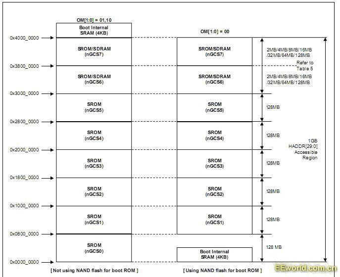
When OM[1:0]=01 or 10: 0x4000_0000-0x4000_0fff. These 4 bytes are the steppingstone mentioned above. 0x4000_0fff_0x4800_0000 is not used. The space of 0x4800_0000-0x6000_0000 is the special function register. You will find that all registers are within this range. 0x6000_0000-0Xffff_ffff is still unused.
When OM[1:0]=00, as shown in the figure above, the steppingstone just mentioned is mapped to ox000_0000, which is the BOOT INTERNAL SRAM on the way. The others are the same.
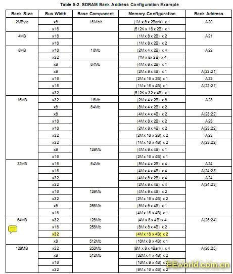
Actually, S3C2440 divides the lower 1G space into 8 blocks. As can be seen from the figure, the starting addresses of the 0th to 6th blocks are unchanged. The address of the seventh segment is variable (its address is determined by how much the sixth block needs, anyway, the sixth and seventh are connected together). The first 6 blocks can be ROM SRAM. The last two blocks can be not only ROM, SRAM, but also SDRAM. Actually, to put it simply, only the last two blocks can be SDRAM. That is to say, SDRAM must be mapped to these two blocks. Mini2440 chooses to map to the seventh block, so the starting address of SDRAM is 0x3000_0000 (this is why the manual sets the initial value of DNW to this when loading the test program, it is to load the program directly to SDRAM, this is just for experiment and it will be lost after power failure. So it is impossible to do this when making products).
I just said that S3C2440 divides the storage space into 8 blocks. Why does it do this? In fact, it is very simple. Even if it does not do this, we will do it. Let's do the math first: 128M per block, that is, 27 address lines are needed for addressing. And 8 blocks are followed by 8 chip select pins corresponding to each one. Speaking of this, smart readers will surely think that these 8 chip select pins are actually decoded by 3 address lines. So a total of 30 address lines are used, and 30 are just 1G. Haha.
That's about it. There should be a lot to be improved, but this is still helpful for beginners, right?
S3C2440 Memory Controller Detailed Explanation
The width of BANK0 bus is determined by OM[1:0] pins. When OM[1:0]=01, the booting ROM data width is 16 bits. When [1:0]=10, the booting ROM data width is 32 bits. When OM[1:0]=00, boot from NAND FLASH. On the Friendly Arm S3C2440 development board, the OM1 pin is directly grounded.


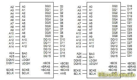
The specific connection method between the S3C2440 and the two SDRAMs is shown in the figure below:

As an ARM engineer, you only need to understand the working timing of SDRAM. The specific read and write control is completed by the register controller. As an FPGA engineer, you need to understand the working principle and timing of SDRAM in detail. I will not go into details here. As an ARM engineer, the most important thing is to accurately configure the registers related to SDRAM.
Software programmable big-endian and small-endian modes;
Address space: Each bank can address 128MB (a total of 8 banks with 1GB space);
Programmable access bit width: BANK0 is 16 or 32 bits, other BANKs are 8, 16 or 32 bits;
8 memory banks, 6 of which are used for ROM or SRAM, and 2 for ROM, SRAM or SDRAM;
The starting address of BANK0~BANK6 is fixed;
The starting address and size of BANK7 are programmable;
The access cycle of all memory banks is programmable;
External wait signal can extend the bus cycle;
Supports SDRAM self-refresh and power-down modes.

Previous article:Learning infrared remote control based on LPC1114
Next article:Why are PC=PC+8 in both ARM3-stage and 5-stage pipelines?
Recommended ReadingLatest update time:2024-11-15 17:50


 Professor at Beihang University, dedicated to promoting microcontrollers and embedded systems for over 20 years.
- LED chemical incompatibility test to see which chemicals LEDs can be used with
- Application of ARM9 hardware coprocessor on WinCE embedded motherboard
- What are the key points for selecting rotor flowmeter?
- LM317 high power charger circuit
- A brief analysis of Embest's application and development of embedded medical devices
- Single-phase RC protection circuit
- stm32 PVD programmable voltage monitor
- Introduction and measurement of edge trigger and level trigger of 51 single chip microcomputer
- Improved design of Linux system software shell protection technology
- What to do if the ABB robot protection device stops
- Keysight Technologies Helps Samsung Electronics Successfully Validate FiRa® 2.0 Safe Distance Measurement Test Case
- Innovation is not limited to Meizhi, Welling will appear at the 2024 China Home Appliance Technology Conference
- Innovation is not limited to Meizhi, Welling will appear at the 2024 China Home Appliance Technology Conference
- Huawei's Strategic Department Director Gai Gang: The cumulative installed base of open source Euler operating system exceeds 10 million sets
- Download from the Internet--ARM Getting Started Notes
- Learn ARM development(22)
- Learn ARM development(21)
- Learn ARM development(20)
- Learn ARM development(19)
- Learn ARM development(14)
- Unboxing of Materials - STM32F767 & ESP32
- Prize Review: 50 Rapid IoT Kits from NXP to Proof of Concept in Minutes
- Download Keysight Technologies' e-book "X-Apps Treasure Map: Essential Measurement Apps for Signal Analyzers That Accelerate Tests" and receive a gift!
- [Evaluation of EC-01F-Kit, the EC-01F NB-IoT development board] Power-on and serial port test
- ELEXCON 2022 Shenzhen International Electronics Exhibition will open on November 6 (new schedule), hurry up and get your tickets! There are also many gifts waiting for you!
- Registration reminder: In the last few hours, 100 sets of Pingtouge RISC-V ecological development boards worth 390 yuan will be given away for free~
- Visit Avnet New Energy Technology Innovation Cloud Exhibition and win great gifts!
- Python Learning Handbook (4th Edition)
- Small Automotive Front-End 16W Power Supply Reference Design
- What is stray capacitance

 Monocular semantic map localization for autonomous vehicles


 京公网安备 11010802033920号