1 Backlight dimming solution
Taking the TFT liquid crystal panel structure as an example, it includes backlight, polarizer, liquid crystal array, color filter and other parts. The display image perceived by the human eye is the comprehensive effect of the above parts. Assume that the backlight brightness is normalized and set to b (a real number in the interval [0,1]), 0 corresponds to the backlight off, and 1 corresponds to the maximum backlight brightness. If the light source is LED , the adjustment of b can include current pulse width modulation, current amplitude adjustment and other methods.
Assuming that the image is an 8-bit grayscale image, f(x,y) represents the grayscale value of a point (x,y) in the image, and x and y are the coordinates of the point. Then the liquid crystal transmittance at the point can be expressed as:
t (x,y)=f(x,y)/255 (1)
The observable brightness L(x,y) of the image point is the combined effect of the backlight luminance and the liquid crystal transmittance, which can be expressed as an approximate linear combination of the backlight brightness b and the liquid crystal transmittance t (x,y):
L(x,y) =b·t (x,y) =b·f(x,y)/255 (2)
According to the requirement of visual light effect consistency, a method must be found to make the pixel gray value as unsaturated as possible when it increases (to compensate for the decrease of backlight b). To achieve this goal, this paper first limits the gray value range of the image to a certain interval, and then stretches the histogram to increase the pixel gray value. The image histogram is clipped by thresholds fgl and fgh, so that some points in the image are clamped at fgl and fgh. The gray interval of the image is limited to [fgl, fgh]. The backlight dimming problem is transformed into how to adjust the image after the histogram is clipped so that its backlight can reduce the brightness as much as possible.
Obviously, for a fixed distortion, fgl and fgh can have multiple values, and the value selection method here should satisfy formula (3):
min (fgh-fgl ) (3)
The purpose of this processing is to limit the grayscale range of the image to a minimum range.
After formula (3) is implemented, the next step is to linearly shift the histogram so that the grayscale moves fgl to the dark area as a whole. In this way, the grayscale area of the image is compressed from the original distribution in the interval [0, 255] to the interval [0, fgh-fgl].
Assuming that the backlight becomes dim, the image should be stretched to compensate for the brightness loss caused by the backlight. If a linear stretching method is used, the maximum stretching multiple is obviously 255/(fgh-fgl). At this time, the pixel grayscale will not be saturated, and the backlight brightness can be reduced from 1 to (fgh-fgl)/255. According to formula (2), the visual effect of the processed image remains unchanged before and after the backlight adjustment.
2 Hardware and software implementation solutions
This experiment uses the mini2440 development board for verification. The mini2440 is a low-cost and practical ARM9 development board with a Samsung S3C2440 processor (ARM920T, with a maximum frequency of 532MHz). The LCD screen supports black and white, 4-level grayscale, 16-level grayscale, 256 colors, and 4,096-color STN LCD display. The size ranges from 3.5 to 12.1in, and the screen resolution can reach 1,024×768 pixels. The experiment uses a 3.5in LED backlight TFT LCD screen.
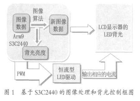
In the experiment, the grayscale value of the image is calculated according to the image algorithm, and the histogram of the displayed image is clipped to limit it to a certain range, and then the histogram is stretched, and then the display brightness of the backlight is calculated by the calculation formula (fgh-fgl)/255, and the duty cycle of the backlight pulse width modulation output pulse is controlled to achieve the brightness adjustment of the backlight LED . The hardware block diagram is shown in Figure 1.

2.1 LED backlight driver design
The design uses a constant current LED driver with a stable output current, ensuring the constant brightness of the backlight LED . It is convenient to determine the output current by changing the relevant peripheral resistors, and has a highly sensitive switch control function, which can control the brightness of the LED through PWM.
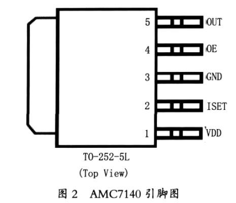
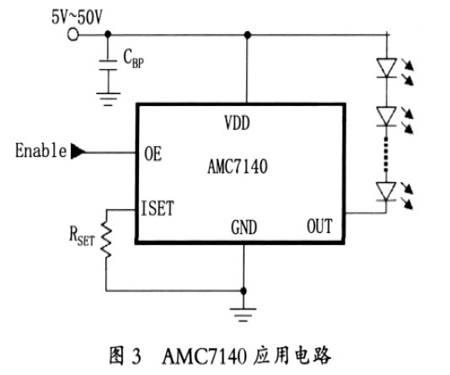
AMC7140 is a high-power LED constant current driver chip with a wide voltage input DC range of 5~50V and a maximum output current of 700mA. It is suitable for driving 1W, 3W, and 5W LED lamps. It is packaged in TO-252-5L and has a PWM CONTROL terminal (OE pin). As shown in Figure 2, it is the pin diagram of AMC7140, where pin 1 is the power input; pin 2 is the control terminal of the output current, and the current is controlled by a high-precision resistor Rset grounded, the current Iset=1.2V/Rset, the output current Iout=500×Iset; pin 3 is grounded; pin 4 is the PWM control terminal, which is valid at high level; pin 5 is the output terminal. The application circuit of AMC7140 is shown in Figure 3.


2.2 Implementation of PWM control based on S3C2440
S3C2440 has 5 16-bit timers. Timers 0, 1, 2, and 3 have pulse width modulation (PWM) function; Timer 4 is an internal timer with no output pins; Timer 0 has a dead zone generator, which is often used in high-current devices; Timers 0 and 1 share an 8-bit pre-pulse divider, and timers 2, 3, and 4 share another one. Each timer has a clock divider that can generate 5 divided signals (1/2, 1/4, 1/8, 1/16, and TCLK). Each timer module gets its clock signal from its own clock divider, which gets its clock from the corresponding 8-bit pre-pulse divider. This 8-bit pre-pulse divider is programmable and divides PCLK according to the values in the TCFG0 and TCFG1 registers. After the timer is enabled, the initial value in the timer count buffer register (TCNTBn) is loaded into the down counter, and the initial value in the timer compare buffer register (TCMPBn) is loaded into the compare register to be compared with the value of the down counter. This double buffering feature of TCNTBn and TCMPBn makes the output signal of the timer more stable when the frequency and duty cycle change. Each timer has its own clock-driven 16-bit down counter. When the counter is reduced to 0, a timer interrupt request is generated to notify the CPU that the timer operation is completed. At the same time, the value of the timer count buffer register is automatically loaded into the down counter again to continue the next operation. However, if the enable bit of the timer TCONn is cleared in normal mode, the value of TCNTBn will no longer be loaded into the counter. The value of TCNTBn is often used for PWM. When the value of the down counter is equal to the value of the compare register, the timer control logic changes the output level. Therefore, the compare register determines the opening and closing of the PWM output.
To set a timer, first initialize TCNTBn and TCMPBn. When initializing the timer, mainly set the following registers (taking timer 0 as an example):
Timer output clock frequency = PCLK/(prescaler value+1)/(divider value)
TCFG0 register setting: TCFG0=99; //prescaler value="99"
TCFG1 register setting: TCFG1=0x03; //divider value="1/16"
Thus, when PCLK=400M, the timer output frequency is 6.25M.
The timer initial value settings include:
TCNTB0 register setting: TCNTB0=62500; // load initial value and interrupt once every 1s
TCMPB0 register setting: TCMPB0=rTCNTB0》1; //50%
Then you can start the timer. The first time you have to load it manually: TCON=1<1;
After loading, change to automatic loading and start the timer: TCON=0x09.
2.3 Image Algorithm Design Based on S3C2440
The S3C2440 chip integrates an LCD controller to transmit image data to the LCD and provide necessary control signals, such as VFRAME, VLINE, VCLK, VM, etc. It can support STNLCD and TFTLCD. The mini2440 uses a 3.5in (resolution of 240×320 pixels) TFT LCD screen, configured in the commonly used 16BPP (5:6:5) mode. To display an image, just write pixel data (R(5):G(6):B(5)) to LCD_BUFFER, and the LCD controller will automatically read the data through DMA and send it to the TFTLCD for display.
The image algorithm is based on the image histogram for data transformation, so first you should write a subroutine and calculate the grayscale histogram of the displayed image. The algorithm is as follows (where bmp is the original grayscale image and bmp_2 is the grayscale value array):
for( y = 0;y < 320;y++ )
{for(x = 0; x < 240; x++)
{bmp_2 [bmp[p]] ++;
p = p + 1;
}
}
Assuming a 5% distortion, the number of pixels that need to be transformed is 240×320×5%=3,840 points. Then, based on the above algorithm principle, a point-by-point calculation method is used to calculate the corresponding (fgh-fgl) starting from grayscale 0, and finally min(fgh - fgl) is obtained by comparison.
The next step is to linearly shift the histogram so that the grayscale moves fgl to the dark area as a whole. In this way, the grayscale area of the image is compressed from the original distribution in the interval [0,255] to the interval [0,fgh-fgl]. Next, the image should be grayscale stretched to compensate for the brightness loss caused by the backlight. If the linear stretching method is adopted, the maximum stretching multiple is obviously 255/(fgh-fgl). The algorithm is as follows (where bmp is the original grayscale image, bmp_new is the updated image, and min= min(fgh - fgl)):
for(y = 0;y < 320;y++)
{for(x = 0;x < 240;x++ )
{if (bmp[p]>= fgl )
bmp_new[p] = (bmp[p] - fgl )*255/min;
else
bmp_new[p] =0;
p++;
}
}
At this time, the pixel grayscale will not be saturated, so the backlight brightness can be reduced from 1 to (fgh-fgl)/255, and the LED drive circuit can achieve corresponding brightness control through PWM.
3 Experimental Results
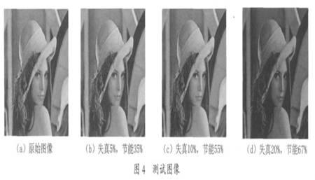
As shown in FIG4 , the test image is shown. FIG4( a ) is the original image, and FIG4( b ), ( c ) and ( d ) are the test result diagrams using the histogram cropping and stretching algorithm.

The distortion of test image 4 (b) is 5%, and the energy saving ratio is 35%; the distortion of test image 4 (c) is 10%, and the energy saving ratio is 55%; the distortion of test image 4 (d) is 20%, and the energy saving ratio is 67%. It can be seen from the experimental results that under a certain distortion, the smaller the grayscale range of histogram clipping, the greater the reduction of backlight brightness. Compared with the original test image after histogram clipping and stretching, under the constraint of 5% distortion, the overall brightness of the image changes due to the histogram shift, but in general, there is no obvious loss in image quality.
4 Conclusion
This paper proposes a power-saving dimming method for LCD backlight based on visual characteristics, establishes a processing framework for histogram cropping and stretching, and verifies it using the ARM platform. It proves that the method in this paper can achieve about 35% backlight power saving effect with a distortion of 5% and there is no obvious loss in image quality.
Previous article:A risk-free path to power system design
Next article:Design of power distribution control module based on LPC2119
- Popular Resources
- Popular amplifiers
- MathWorks and NXP Collaborate to Launch Model-Based Design Toolbox for Battery Management Systems
- STMicroelectronics' advanced galvanically isolated gate driver STGAP3S provides flexible protection for IGBTs and SiC MOSFETs
- New diaphragm-free solid-state lithium battery technology is launched: the distance between the positive and negative electrodes is less than 0.000001 meters
- [“Source” Observe the Autumn Series] Application and testing of the next generation of semiconductor gallium oxide device photodetectors
- 采用自主设计封装,绝缘电阻显著提高!ROHM开发出更高电压xEV系统的SiC肖特基势垒二极管
- Will GaN replace SiC? PI's disruptive 1700V InnoMux2 is here to demonstrate
- From Isolation to the Third and a Half Generation: Understanding Naxinwei's Gate Driver IC in One Article
- The appeal of 48 V technology: importance, benefits and key factors in system-level applications
- Important breakthrough in recycling of used lithium-ion batteries
- LED chemical incompatibility test to see which chemicals LEDs can be used with
- Application of ARM9 hardware coprocessor on WinCE embedded motherboard
- What are the key points for selecting rotor flowmeter?
- LM317 high power charger circuit
- A brief analysis of Embest's application and development of embedded medical devices
- Single-phase RC protection circuit
- stm32 PVD programmable voltage monitor
- Introduction and measurement of edge trigger and level trigger of 51 single chip microcomputer
- Improved design of Linux system software shell protection technology
- What to do if the ABB robot protection device stops
- CGD and Qorvo to jointly revolutionize motor control solutions
- CGD and Qorvo to jointly revolutionize motor control solutions
- Keysight Technologies FieldFox handheld analyzer with VDI spread spectrum module to achieve millimeter wave analysis function
- Infineon's PASCO2V15 XENSIV PAS CO2 5V Sensor Now Available at Mouser for Accurate CO2 Level Measurement
- Advanced gameplay, Harting takes your PCB board connection to a new level!
- Advanced gameplay, Harting takes your PCB board connection to a new level!
- A new chapter in Great Wall Motors R&D: solid-state battery technology leads the future
- Naxin Micro provides full-scenario GaN driver IC solutions
- Interpreting Huawei’s new solid-state battery patent, will it challenge CATL in 2030?
- Are pure electric/plug-in hybrid vehicles going crazy? A Chinese company has launched the world's first -40℃ dischargeable hybrid battery that is not afraid of cold
- Switching power supply waveform
- [Raspberry Pi 4B Review] + Real-time status monitoring website test service resource usage
- The latency of cache in arm system refers to
- 【W806 Lianshengde Development Board】Real-time performance
- CC1352R SimpleLink High-Performance Dual-Band Wireless MCU
- Electric race, how are you guys doing?
- Howland's improved circuit output resistance
- Ov7670 image acquisition source program based on TINYM0 LPC1114
- Pingtouge Scenario-based Bluetooth Mesh Gateway Program Burning
- How to improve the anti-interference (radiation) ability of operational amplifiers

 5962-9755701HPA


 京公网安备 11010802033920号