As energy crisis and climate warming become more and more serious, energy conservation and environmental protection have become the focus of social issues. LED has attracted widespread attention due to its high efficiency, energy saving, environmental protection, long life, rich colors, small size, flicker resistance, high reliability, easy control and many other advantages. It is considered to be the most promising lighting source in the 21st century. Traditional incandescent lamps have low efficiency and high power consumption; fluorescent lamps save electricity, but have short service life, are fragile, and waste has mercury pollution; high-intensity gas discharge lamps have disadvantages such as low efficiency, high power consumption, short life, and electromagnetic radiation hazards; if LED lighting can replace the current low-efficiency, high-energy-consuming traditional lighting, it will undoubtedly alleviate the current increasingly urgent energy shortage and environmental deterioration problems. Due to the volt-ampere characteristics and temperature characteristics of LED itself, the sensitivity of LED to current is higher than that to voltage, so it cannot be directly powered by traditional power supply. Therefore, to use LED as a lighting source, the problem of power drive must be solved first. Although the traditional LED driver power supply can realize LED brightness adjustment, it cannot realize power factor correction, the input power factor is relatively low, and the harmonics are relatively large. In order to make the input current harmonics of the LED driver meet the requirements, power factor correction must be added. This article introduces a single-stage PFC flyback LED power supply, which uses fewer components, has low losses, and has a higher power factor and efficiency.
1 Circuit Principle Analysis
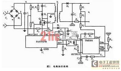
Figure 1 is a simplified circuit diagram. The circuit adopts a single-stage flyback topology, consisting of full-wave rectification, DC/DC conversion, output rectification and filtering circuit, error feedback circuit, and PWM controller circuit.

FAN7527B is an active power factor correction control chip launched by Fairchild Semiconductor. The excellent performance of the multiplier circuit inside the chip can be used in applications with a wide AC mains input voltage range (85~265VAC). And the THD value of the circuit is very small, so as to obtain a good active power factor correction control function. Its startup working current is only tens of microamperes, and the circuit shutdown control function can be realized by using its zero current detection FAN7527B's 5th pin.
The input capacitor of the circuit has a very small capacity (i.e. the output filter capacitor capacity of the AC input mains rectification is very small), so the maximum input voltage of the APFC circuit is very close to the peak value of the output voltage after the AC input mains voltage is rectified. The main advantage of this circuit is its high power factor (generally greater than 0.92), which can well meet the technical requirements of EMC and THD, especially in applications with a wide AC mains input voltage range. In applications with heavy output loads, the circuit can achieve higher working efficiency, generally close to 90%. Working in the current critical conduction mode can make the conduction loss of the APFC power switch MOSFET relatively small, which is conducive to reducing the size of the heat sink.
The voltage on C1 in the figure is the voltage after bridge rectification. Rs1 samples the current flowing through the MOS tube and performs cycle-by-cycle current limiting control to prevent the current peak of the MOS tube from being too large, ensuring that the transformer does not experience magnetic saturation when the load is short-circuited. The auxiliary winding is used to complete the current zero-crossing detection of the primary winding of the transformer (APFC transformer demagnetization), and the power switch tube Q2 is controlled to restart the next switch conduction cycle. The resistance value of the resistor R4 connected to the Idet pin of FAN7527B is in the range of tens of kilo-ohms, so that the circuit works in the "quasi-zero voltage conduction" mode. The resistance value of R4 is related to the inductance of the primary winding of the transformer and the output capacitance of the power switch tube MOSFET. The specific resistance value can be determined through experiments. In this circuit, the value is 33K. Rs2 samples the load LED current signal, and R7 and R8 form a voltage divider network to sample the voltage on the LED. Rs2 samples the current on the LED and compares it with the reference signal CVin on TM101. The output is controlled by the error amplifier. The brightness of the LED is basically proportional to the current flowing through the LED. The brightness of the LED can be adjusted by controlling the current flowing through the LED. R7 and R8 sample the voltage on the LED and compare it with the reference signal CVin on TM101. The output voltage is controlled by the error amplifier. The two signals sent to TM101 are "ANDed" and sent to the error amplifier of the control chip FAN75 27B through the optical coupler to enter the multiplier. The other way of the multiplier is to sample the full-wave rectified AC signal through R13, R19, R23 and R27. The product of these two signals is the output of the multiplier. The output signal makes the inductor current track the output waveform signal of the multiplier. The generated PWM pulse controls the switch of the MOS tube Q1 to control the load current and input current, and complete the constant current and voltage limiting control of the LED and the correction of the input power factor.
2 Transformer parameter calculation
The transformer is one of the core components of the power supply. The performance of the transformer not only affects the heat generation and efficiency of the transformer itself, but also affects the technical performance and reliability of the switching power supply. Therefore, during the design and production, the selection of core materials, the structure of the core and coil, and the winding process must be carefully considered.
Design parameters: ①fs=80-120kHz, Bs=0.2T, D=0.45; ②AP=Ae×Aw=1.82cm4; ③Input and output voltage: Vin=176~264VAC; Vout=176~264VAC;=36V; ④Output current: Io=3.8A, ⑥Circuit form: flyback, the transformer uses PC40 PQ32/25 core.
(1) Transformer parameter calculation
Transformer design output capability
Among them, the current density δ=300A/cm2, the output power PT=136W, and the window duty factor Kw=0.4.
The actual output capacity of the transformer is AP = Ae × Aw = 0.55 cm4, and the magnetic core meets the design requirements. (2) Calculate the peak current of the primary and secondary
(3) Calculate primary inductance and air gap length
Primary inductance
Air gap length(mm)
Where △B is the change in magnetic flux density, △B=0.805BS+125GS=1730GS-0.173T, where the unit is mT.
(4) Calculate the number of turns of the transformer winding
a Changes in the number of primary and secondary turns

b Primary winding turns: The number of turns of the primary winding
The resulting number of turns is 21 turns.
c Number of turns of the secondary winding
The output voltage is 36V, so the secondary output turns N22=N21=N1/n=75/12.5=6, so 6 turns are taken.
3 Test results
According to the above analysis, a 120W output power prototype was made for testing. The input voltage of the prototype was AC 220V, and the output current was constant 3.5A. The main parameters of the circuit were: error amplifier compensation parameters: C4=1μF, R5=63K, R11=47K; output capacitor C6=3300μF, and the power tube was 17N80C3 from Fairchild Semiconductor.
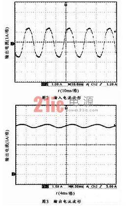
Figure 2 is the input current waveform measured when the input is 220V and the output is fully loaded at 120W. It can be seen that the input current is close to a standard sine wave and the measured power factor reaches 0.977.
Figure 3 shows the output current waveform when the input is 220V and the output is fully loaded. The peak-to-peak value of the ripple current is 120mA, and the output current is superimposed with a ripple current of twice the mains supply frequency.

4 Conclusion
This article introduces a single-stage flyback power factor correction LED driver with FAN7527B as the core. Compared with LED drivers of the same power level, its main advantage is its high power factor (generally greater than 0.95), which can well meet the technical requirements of electromagnetic compatibility and current harmonic components, especially in applications with a wide AC input voltage range. In applications with heavy output loads, the circuit has high efficiency (greater than 0.88) and low heat generation, which reduces damage to LED lamp holders.
Previous article:Hysteresis control to achieve constant current LED drive
Next article:Analysis of 75W Flyback LED Driver Power Supply Circuit
- Popular Resources
- Popular amplifiers
- MathWorks and NXP Collaborate to Launch Model-Based Design Toolbox for Battery Management Systems
- STMicroelectronics' advanced galvanically isolated gate driver STGAP3S provides flexible protection for IGBTs and SiC MOSFETs
- New diaphragm-free solid-state lithium battery technology is launched: the distance between the positive and negative electrodes is less than 0.000001 meters
- [“Source” Observe the Autumn Series] Application and testing of the next generation of semiconductor gallium oxide device photodetectors
- 采用自主设计封装,绝缘电阻显著提高!ROHM开发出更高电压xEV系统的SiC肖特基势垒二极管
- Will GaN replace SiC? PI's disruptive 1700V InnoMux2 is here to demonstrate
- From Isolation to the Third and a Half Generation: Understanding Naxinwei's Gate Driver IC in One Article
- The appeal of 48 V technology: importance, benefits and key factors in system-level applications
- Important breakthrough in recycling of used lithium-ion batteries
- LED chemical incompatibility test to see which chemicals LEDs can be used with
- Application of ARM9 hardware coprocessor on WinCE embedded motherboard
- What are the key points for selecting rotor flowmeter?
- LM317 high power charger circuit
- A brief analysis of Embest's application and development of embedded medical devices
- Single-phase RC protection circuit
- stm32 PVD programmable voltage monitor
- Introduction and measurement of edge trigger and level trigger of 51 single chip microcomputer
- Improved design of Linux system software shell protection technology
- What to do if the ABB robot protection device stops
- Allegro MicroSystems Introduces Advanced Magnetic and Inductive Position Sensing Solutions at Electronica 2024
- Car key in the left hand, liveness detection radar in the right hand, UWB is imperative for cars!
- After a decade of rapid development, domestic CIS has entered the market
- Aegis Dagger Battery + Thor EM-i Super Hybrid, Geely New Energy has thrown out two "king bombs"
- A brief discussion on functional safety - fault, error, and failure
- In the smart car 2.0 cycle, these core industry chains are facing major opportunities!
- The United States and Japan are developing new batteries. CATL faces challenges? How should China's new energy battery industry respond?
- Murata launches high-precision 6-axis inertial sensor for automobiles
- Ford patents pre-charge alarm to help save costs and respond to emergencies
- New real-time microcontroller system from Texas Instruments enables smarter processing in automotive and industrial applications
- Is it necessary to pull up the data line and pull down the clock line in SWD mode for the burning port?
- [RVB2601-demo analysis and kernel analysis] YOC architecture + three-color indicator light
- dsp2812 ADC application experience
- The questions for this national competition were released at 7:30 this morning. What do you think?
- [Ateli Development Board AT32F421 Review] -TEST03 ADC Test
- The talented photographer photographed 150 countries in 10 years, capturing the ultimate beauty of Chinese ink painting and astonishing the world!
- Can a multi-turn potentiometer be used for direction detection?
- SHT31 evaluation + mobile phone APP connection successful
- How to learn Altera Cyclone IV
- si114x infrared sensor

 LMC6082AMN


 京公网安备 11010802033920号