LEDs are expected to transform the lighting industry with their long life and low power consumption, but the main barrier to their rapid adoption is the high cost of the LEDs themselves. The cost of LED luminaires (complete electric lighting equipment) varies, but the cost of LEDs typically accounts for about 25% to 40% of the total luminaire cost and is expected to remain a high percentage for many years to come (Figure 1).
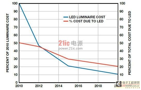
Figure 1. LED luminaire cost breakdown1
One way to reduce the overall fixture cost is to drive the LED at the highest possible DC current within the product specifications. This current may be much higher than its "binning current". If driven properly, this may produce a higher lumen/cost ratio.
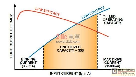
Figure 2. LED light output and efficiency vs. drive current2
However, this approach requires a higher current driver. There are many solutions that drive LEDs at low currents (<500mA), but there are few options for higher currents (700mA to 4A). This may seem surprising, as the semiconductor industry has a large number of DC-DC solutions with capabilities up to 4A, but they are designed to control voltage, not LED current. This article will explore some simple techniques for converting an off-the-shelf DC-DC buck regulator into a smart LED driver.
The buck regulator chops the input voltage and passes it through an LC filter to provide a regulated output, as shown in Figure 3. It uses two active components and two passive components. The active components are the switch "A" from the input to the inductor, and the switch (or diode) "B" from ground to the inductor. The passive components are the inductor (L) and the output capacitor (COUT) which form an LC filter that reduces the ripple generated by the active components.
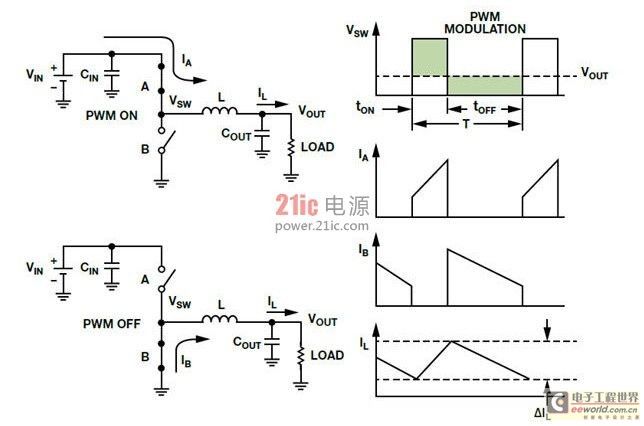
Figure 3. Basic buck scheme.
If the switches are internal, the buck is called a regulator, and if the switches are external, it is called a controller. If both switches are transistors (MOSFETs or BJTs), it is synchronous, and if the bottom switch is implemented using a diode, it is asynchronous. Each of these types of buck circuits has advantages and disadvantages, but synchronous buck regulators can usually optimize efficiency, part count, solution cost, and board area. Unfortunately, synchronous buck regulators for driving high current LEDs (up to 4A) are rare and expensive. This article uses the ADP2384 as an example to show how to modify the connections of a standard synchronous buck regulator to regulate LED current.
The ADP2384 high-efficiency synchronous buck regulator specifies output currents up to 4 A with input voltages up to 20 V. Figure 4 shows the normal connections for regulating the output voltage.
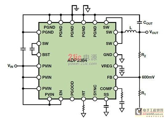
Figure 4. ADP2384 connected for output voltage regulation.
In operation, the divided output voltage is connected to the FB pin, compared to the internal 600 mV reference, and used to generate the appropriate duty cycle for the switch. In steady state, the FB pin is held at 600 mV, so VOUT is regulated to 600 mV times the divider ratio. If the upper resistor is replaced by an LED (Figure 5), the output voltage must be whatever value is needed (within the ratings) to maintain FB at 600 mV; therefore, the current through the LED is controlled to 600 mV/RSENSE.
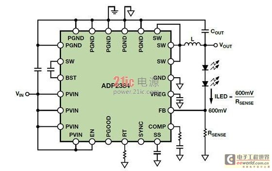
Figure 5. Basic (but inefficient) LED driver
This circuit works well when a precision resistor from FB to ground sets the LED current, but the resistor dissipates a lot of power: P = 600 mV × ILEDFor low LED currents, this is not a big problem, but at high LED currents, the inefficiency can significantly increase the heat dissipated by the lamp (600 mV × 4 A = 2.4 W). Reducing the FB reference voltage can reduce power dissipation proportionally, but most DC-DC regulators do not have a way to adjust this reference. Fortunately, two tricks can reduce the reference voltage of most buck regulators: use the SS/TRK pin-or offset the RSENSE voltage.
Many general-purpose buck ICs include a soft-start (SS) or tracking (TRK) pin. The SS pin slowly increases the switch duty cycle at startup, minimizing startup transients. The TRK pin allows the buck regulator to follow an independent voltage. These functions are often combined into a single SS/TRK pin. In most cases, the error amplifier compares the minimum of the SS, TRK, and FB voltages to a reference, as shown in Figure 6.
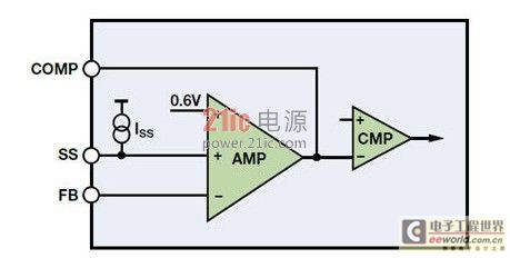
Figure 6. Operation using the soft start pin of the ADP2384.
For lamp applications, set the SS/TRK pin to a fixed voltage and use it as the new FB reference. Constant voltage dividers work very well as reference sources. For example, many buck regulator ICs include a controlled low voltage output—such as the VREG pin on the ADP2384. For even greater accuracy, a simple 2-pin external precision reference can be used, such as the ADR5040. In any case, a resistor divider from this supply to the SS/TRK pin forms the new reference voltage. Setting this voltage between 100 mV and 200 mV generally provides the best balance between power dissipation and LED current accuracy. Another advantage of a user-selected reference voltage is that RSENSE can be selected to a convenient standard value, thus avoiding the expense and inaccuracy of specifying or assigning arbitrary precision resistor values to set the LED current.
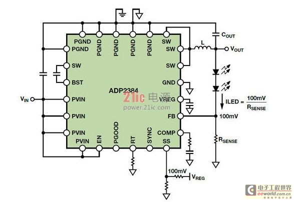
Figure 7. Using the SS/TRK pin to reduce the FB reference voltage.
Using the SS or TRK pin approach is not feasible for all buck regulators, as some ICs do not have these pins. Also, for some buck ICs, the SS pin changes the peak inductor current instead of the FB reference, so the product data sheet must be carefully reviewed. As an alternative, an RSENSE voltage offset can be generated. For example, a resistor divider between a precision voltage source and RSENSE provides a fairly constant offset voltage from RSENSE to the FB pin (Figure 8).
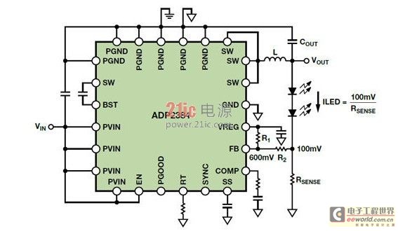
Figure 8. Generating RSENSE voltage offset
The required value of the resistor divider can be calculated using Equation 1, where VSUP is the auxiliary regulation voltage and FBREF(NEW) is the target voltage across RSENSE.

Therefore, the effective feedback reference of 150 mV can be obtained using the following formula, where R2 = 1 kΩ and VSUP = 5 V:

The LED current is:

This method does not require the SS or TRK pins. The FB pin still regulates to 600 mV (but the voltage at RSENSE is regulated to FBREF(NEW)). This means that the other functions of the chip (including soft-start, tracking, and power good indication) will still operate normally.
The disadvantage of this approach is that the offset between RSENSE and FB is severely affected by the accuracy of the power supply. Using a precision voltage reference such as the ADR5040 may be ideal, but a less precise ±5% reference tolerance may produce a ±12% change in the LED current. Table 1 shows the comparison:
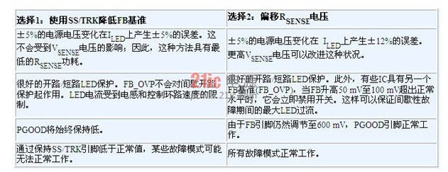
Table 1. Comparison of SS/TRK and offset RSENSE
Another key to accurate current regulation is proper layout of the connections to the sense resistor. A 4-lead sense resistor is ideal but can be expensive. With good layout techniques, we can achieve high accuracy using a traditional 2-lead resistor as shown in Figure 9.
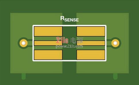
Figure 9. Recommended PCB routing for RSENSE
Functions other than adjustment
Regulating LED current is very simple using an off-the-shelf buck regulator. The example here uses the ADP2384. The more detailed paper also includes examples using the ADP2441, which has fewer pins and a 36 V input voltage range. It shows examples of how to implement many of the “smart” features offered by dedicated LED buck regulators, such as LED short/open fault protection, RSENSE open/short fault protection, PWM dimming, analog dimming, and current foldback thermal protection. In this article, we will use the ADP2384 from the example above and discuss PWM and analog dimming, current foldback.
Dimming using PWM and analog control
A key requirement for a "smart" LED driver is to use dimming to adjust LED brightness, using one of two methods: PWM and analog. PWM dimming controls the LED current by adjusting the duty cycle of the pulses. If the frequency is above 120 Hz, the human eye will average these pulses to produce a perceptible average light level. Analog dimming regulates the LED current at a constant DC value.
PWM dimming can be implemented by turning on and off an NMOS switch inserted in series with RSENSE. These current levels may require a power device, but adding a power device would offset the size and cost benefits gained by using a buck regulator that includes its own power switch. Alternatively, PWM dimming can be performed by rapidly turning the regulator on and off. At low PWM frequencies (<1 kHz), this still provides good accuracy (Figure 10).
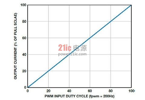
Figure 10. ADP2384 PWM Dimming Linearity—Output Current vs. Duty Cycle at 200 Hz
Like all general-purpose buck regulators, the ADP2384 does not have a pin to apply a PWM dimming input, but the FB pin can be manipulated to enable and disable switching. If FB goes high, the error amplifier goes low and the buck switching stops. If FB is reconnected to RSENSE, it will resume normal regulation. This can be achieved with a low-current NMOS transistor or a general-purpose diode. In Figure 11, a high PWM signal connects RSENSE to FB, achieving LED regulation. A low PWM signal turns off the NMOS, and there is a pull-up resistor to bring the FB level to a high level.
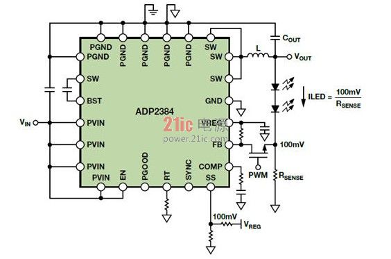
Figure 11. PWM dimming using the ADP2384.
Although PWM dimming is very popular, sometimes we need noise-free “analog” dimming. Analog dimming simply regulates a constant LED current, while PWM dimming performs chopping. If two dimming inputs are used, analog dimming is required because multiple PWM dimming signals may produce a beat frequency, resulting in flicker or audible noise. However, it is possible to use PWM for one dimming control and analog for the other. Using a general-purpose buck regulator, the simplest way to implement analog dimming is to control the FB reference by adjusting the supply to the FB reference circuit, as shown in Figure 12.
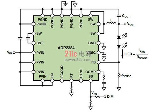
Figure 12. Analog dimming circuit
Thermal Foldback
Because the life of an LED depends largely on its operating junction temperature, it is sometimes necessary to monitor the LED temperature and respond if it gets too high. Abnormally high temperatures can be caused by improper heat sink connections, excessive ambient temperatures, or some other extreme condition. A common solution is to reduce the LED current when the temperature exceeds a certain threshold (Figure 13). This is called LED thermal foldback.
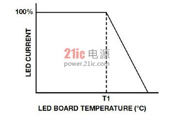
Figure 13. Required LED thermal foldback curve
In this type of dimming, the LED is held at full load current until a temperature threshold (T1) is reached, above which the LED current begins to decrease as the temperature increases. This limits the junction temperature of the LEDs, preserving their useful life. Low-cost NTC (negative temperature coefficient) resistors are often used to measure the heat sink temperature of the LEDs. With minor modifications to the analog dimming scheme, the temperature of the NTC can easily control the LED current. If the SS/TRK pin is used to control the FB reference, a simple method can be used to place the NTC in parallel with the reference voltage (Figure 14).
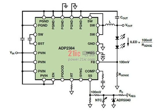
Figure 14. LED thermal foldback using SS/TRK
As the heat sink temperature increases, the NTC resistance decreases. The NTC forms a resistor divider with R3. If the voltage of the voltage divider is higher than the reference voltage, the maximum current is output; if the NTC resistor voltage drops below the reference voltage and then drops below the FB reference voltage, the LED current begins to decrease.
in conclusion
These tips should serve as a general guideline for implementing full LED functionality using a standard buck regulator. However, because these features are a bit outside the target application range of buck ICs, it is best to contact the semiconductor manufacturer to confirm that the IC can handle these operating modes.
Previous article:Brief analysis of LED driver power supply performance characteristics and requirements
Next article:Design and implementation of a centralized LED street light power supply
Recommended ReadingLatest update time:2024-11-15 23:24


- Popular Resources
- Popular amplifiers
-
 MCU C language programming and Proteus simulation technology (Xu Aijun)
 -
 100 Examples of Microcontroller C Language Applications (with CD-ROM, 3rd Edition) (Wang Huiliang, Wang Dongfeng, Dong Guanqiang)
 -
 Research on three-phase all-solid-state high-efficiency LED tunnel lighting system based on chip drive_Li Jian
 -
 Follow me Season 2 Episode 1 All Code + Library
- MathWorks and NXP Collaborate to Launch Model-Based Design Toolbox for Battery Management Systems
- STMicroelectronics' advanced galvanically isolated gate driver STGAP3S provides flexible protection for IGBTs and SiC MOSFETs
- New diaphragm-free solid-state lithium battery technology is launched: the distance between the positive and negative electrodes is less than 0.000001 meters
- [“Source” Observe the Autumn Series] Application and testing of the next generation of semiconductor gallium oxide device photodetectors
- 采用自主设计封装,绝缘电阻显著提高!ROHM开发出更高电压xEV系统的SiC肖特基势垒二极管
- Will GaN replace SiC? PI's disruptive 1700V InnoMux2 is here to demonstrate
- From Isolation to the Third and a Half Generation: Understanding Naxinwei's Gate Driver IC in One Article
- The appeal of 48 V technology: importance, benefits and key factors in system-level applications
- Important breakthrough in recycling of used lithium-ion batteries
- LED chemical incompatibility test to see which chemicals LEDs can be used with
- Application of ARM9 hardware coprocessor on WinCE embedded motherboard
- What are the key points for selecting rotor flowmeter?
- LM317 high power charger circuit
- A brief analysis of Embest's application and development of embedded medical devices
- Single-phase RC protection circuit
- stm32 PVD programmable voltage monitor
- Introduction and measurement of edge trigger and level trigger of 51 single chip microcomputer
- Improved design of Linux system software shell protection technology
- What to do if the ABB robot protection device stops
- Allegro MicroSystems Introduces Advanced Magnetic and Inductive Position Sensing Solutions at Electronica 2024
- Car key in the left hand, liveness detection radar in the right hand, UWB is imperative for cars!
- After a decade of rapid development, domestic CIS has entered the market
- Aegis Dagger Battery + Thor EM-i Super Hybrid, Geely New Energy has thrown out two "king bombs"
- A brief discussion on functional safety - fault, error, and failure
- In the smart car 2.0 cycle, these core industry chains are facing major opportunities!
- The United States and Japan are developing new batteries. CATL faces challenges? How should China's new energy battery industry respond?
- Murata launches high-precision 6-axis inertial sensor for automobiles
- Ford patents pre-charge alarm to help save costs and respond to emergencies
- New real-time microcontroller system from Texas Instruments enables smarter processing in automotive and industrial applications
- Qorvo Online Design Conference - How Antenna Evolution Supports 5G Mobile Devices
- Audio Hardware Basics
- Is there any chip suitable for LED color temperature adjustment that can achieve stepless adjustment of LED color temperature?
- Is the 485 on the development board automatically sending and receiving?
- IAI Servo Cylinder Driver Disassembly
- The advantages of series resonance are becoming more and more prominent
- [Practical Tips!] How to choose an antenna? Remember these points and don’t make the wrong choice!
- Awesome MicroPython
- 8T245
- Comparison and selection of SX1268, SX1278 and SX1276

 MCU C language programming and Proteus simulation technology (Xu Aijun)
 Follow me Season 2 Episode 1 All Code + Library


 京公网安备 11010802033920号