For some power devices (power transistors, VDMOS, IGBT, etc.), by regularly powering on and off the components and applying electrical stress and thermal stress cyclically, their ability to withstand cyclic stress can be tested. Based on the above principle, with the help of the visual programming language LabVIEW and the NI series sb RIO-9612 board, this paper designs a transistor aging test system, which meets the test requirements of the national military standard GJB1036. The sampling time of each station is no more than 4μs, and the sampling cycle of a total of 64 stations is no more than 300μs, which meets the requirements of fast control while maintaining accuracy. The sampling resolution of voltage and current reaches 12 bits, and the accuracy reaches 1%, thereby controlling the junction temperature error of the device. At present, the system has been delivered and put into operation, and the experimental results have met the needs of users and have high practical value.
With the increasing requirements for the quality of electronic products in the fields of aviation, aerospace, energy industry, etc., the reliability of electronic products has received more and more attention. Electronic products will encounter different environmental conditions during use. Under the stress of thermal expansion and contraction, electronic components with poor thermal matching ability are prone to failure, resulting in electronic product failures and huge manpower and financial losses. The aging test of electronic components is to imitate or equivalent the use status of products. Through testing, non-compliant devices are eliminated, and the quality of electronic products is effectively controlled in the early stage of processing to ensure the reliability and stability of electronic products.
In view of this situation of electronic components, we have developed an aging test system that can mainly target power devices (power transistors, VDMOS, IGBT, etc.). By regularly powering on and off the components, cyclically applying electrical stress and thermal stress, and testing their ability to withstand cyclic stress.
1 Working principle
By powering on and heating the transistor, the transistor works at the current constant power. After a period of time, the junction temperature of the device continues to rise due to the heat of the transistor. After reaching the set value, the constant current source and constant voltage source are disconnected, and the device is ventilated to reduce its temperature to the set value. By repeating this process, the heating time and cooling time of the device can be calculated more accurately, achieving the purpose of intermittent testing. The basic working principle diagram is shown in Figure 1.
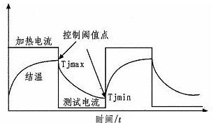
Figure 1 Schematic diagram of intermittent life test cycle
The thermal resistance of semiconductor devices is usually defined as:

Where RθJX = thermal resistance from device junction to specific environment (alternative symbol is θJX) [℃/W];
TJ = device junction temperature under steady-state test conditions [℃];
TX = reference temperature of the environment [℃];
PH = device power consumption [W];
The device junction temperature under test conditions can be expressed as:
Tj = TJ0 + △TJ
Where TJ0 = initial junction temperature before device heating [℃];
△TJ = device junction temperature change The
junction temperature change is expressed by temperature sensitive parameter (TSP), the formula is:
△TJ = K × △TSP
Where △TSP = temperature sensitive parameter change [mV];
K = constant defining the relationship between TJ and TSP change [℃/mV];
The temperature sensitive parameter can be expressed as:
TSP = Ie × -4Vce
Where Ie = constant current source value added at the time of cooling measurement [mV];
Vce = device junction voltage value [mV];
The K coefficient is the relationship between the junction temperature and the junction voltage. The fixed device K coefficient is a constant. The K coefficient of different devices is different. It can be found in the data of the test device or given by the manufacturer. Its calculation formula can be expressed as:

Where TJ1 and TJ2 are the junction temperatures at two moments, and Vce1 and Vce2 are the junction voltages corresponding to the junction temperatures.
2 System Architecture
The system adopts the structure of PC + sbRIO-9612 + main control board + driver board + aging board, as shown in Figure 2. The PC and 9612 communicate through the network port, and the 9612 and the main control board communicate through the digital I/O port. The power supply of sbRIO-9612, main control board, and driver board is completed by the switching regulated power supply. The programmable power supply provides working power for the devices on the aging board. The 16-channel differential AD is used to collect the current, voltage, power supply temperature and other signals of the devices to be tested on the aging board. The system uses sbRIO-9612 plus an expansion board to form a lower computer as the main control board of the system; the main control board and the driver board use bus communication. The main function of the driver board is to convert the 20 pairs of differential signals from the main control board (hardware implementation) to the driver board FPGA, and use 20 signals to communicate with sbRIO-9612. sbRIO-9612 controls the registers in the FPGA to realize the on and off of the power supply, constant current source, and drain/source, thereby establishing power circulation and appropriate sampling conditions. The hardware schematic diagram is shown in Figure 3.
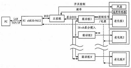
Figure 2 System overall architecture diagram
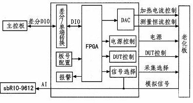
Figure 3 FPGA hardware schematic diagram
The driver board and the aging board are connected by two docking sockets respectively, and the current and voltage sampling signals are transmitted back to the sbRIO-9612 board for AD conversion and then sent to the upper computer.
[page]
3 Workflow and implementation
3.1 Introduction to LabVIEW
LabVIEW is a program development environment. It uses the graphical programming language G to create source programs in the flow chart. The LabVIEW FPGA module extends the LabVIEW graphical development platform to the field programmable gate array (FPGA) on the hardware platform based on the NI reconfigurable I/O (RIO) architecture.
3.2 Workflow
At the beginning of the work, the host computer sends the control command to sbRIO-9612 according to the TCP/IP protocol. After receiving the command, according to the operation of the host computer, sbRIO-9612 sends the corresponding command and related parameters to the main control board. The main control board controls the driver board to execute the command, and then controls the aging board to perform related operations.
sbRIO-9612 is mainly composed of two parts, namely the FPGA part and the RT part; in the division of work, due to the system's requirements for speed, the fan control, programmable power supply control, temperature frequency reading, ADC acquisition, DAC transmission, differential data transmission and other modules are assigned to the fast FPGA part for execution, while the slower RT part mainly realizes the analysis of the host computer instructions, the aging work control and the data transmission from the lower computer to the upper computer. The LabVIEW FPGA workflow diagram is shown in Figure 4.
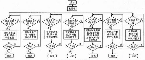
Figure 4 FPGA workflow diagram
3.3 Implementation of the working process
3.3. 1 Overview
Before the work starts, first connect to the lower computer. After the connection is successful, call the self-test module to perform self-test on the aging board to be tested. After the self-test is successful, the upper computer sends the parameters to the lower computer, and then sends the start control command. The lower computer polls the control command word of each board. After the board starts working, the heating current, measurement current, and programmable voltage required for the work are sent to the driver board through the serial data transmission module, and loaded to the corresponding aging board through the driver board. Heat the device and record the time at this time, which is the heating start time. When the difference between the current time and the heating start time is greater than or equal to the on time, stop heating, turn on the fan, record the heating end time, start AD acquisition, calculate the junction temperature based on the collected current and voltage, and send the value back to the upper computer. The upper computer draws a curve based on the temperature change. When the difference between the current time and the heating end time is greater than or equal to the off time, the cooling is completed and the measurement ends, and the next cycle is entered. After the number of cycles is reached, the board is placed in an idle state.
3.3.2 Accuracy and switching speed
1) High-speed ADC acquisition
SbRIO-9612 is integrated with AD acquisition chip. The 16-bit AD can ensure that its sampling resolution reaches 1‰. At the same time, the conversion time of 4μs ensures the sampling speed of AD. In order to eliminate the influence of common mode noise, 32 ADs are converted into 16 differential inputs. During the acquisition, 8 values are taken continuously for each channel each time to calculate the average value as the result of this acquisition. At the same time, the high-speed switch used in the aging board is used for switching to ensure the accuracy of the collected data. The following figure shows the junction voltage of the current NMOS tube (model IRFP460) and the junction temperature of the tube measured at the current moment through LabVIEW at the set measurement current of 10 mA and the programmable voltage of 12 V. The room temperature is 17.3 20 6 degrees Celsius obtained by the temperature sensor installed on each aging board. As can be seen from Figure 5, the values of the 16 channels collected by AD all begin to fluctuate after the third decimal point, ensuring that the calculated △Vf value begins to fluctuate after the second decimal point.
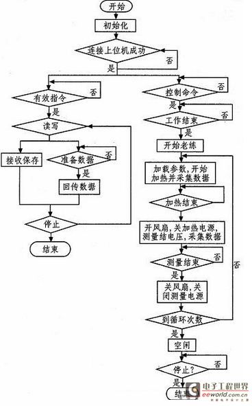
Figure 5 RT workflow diagram
The system can complete the acquisition of all station junction voltages within 20μs after switching from the heating state to the measurement state. In order to meet the requirements of fast acquisition, when writing the program, considering the high real-time performance of ADC, the acquisition part is assigned to the FPGA of sbRIO-9612. The Onboard Clock of sbRIO-9612 is 40 MHz, that is, a period of 0.025μs. When writing the FPGA program, the ADC acquisition configuration (that is, the switch switching command execution) and the acquisition data are placed between two adjacent frames of the sequence structure. Considering the switch switching time, a 1μs wait is added in the middle to ensure the reliability of the data, and then the data acquisition is started. The ADC acquisition part of the program is shown in Figure 6. [page]
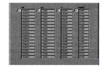
Figure 6 AD acquisition results displayed in LabVIEW

Figure 7 ADC junction voltage acquisition program on FPGA
2) Differential data transmission
This module realizes the communication between sbRIO-9612 and FPGA. The communication mode is bus asynchronous access mode. Data is sent and received through serial DAC mode. The so-called serial DAC means that under a certain clock (clock cycle is 80 MHz), serial data is sent according to a fixed timing. First, the address is assigned to the port. The address is a total of six bits, namely A0-A5. The upper four bits are the address bits (control board number) and the lower two bits are the driver board register address; then the data is placed on the data bus. The data format is U8, set WR/RD high, then: DR is low, keep two clock cycles, DR is high, and the serial DAC writes data; similarly, when reading data, the address bus is set first, WR/RD is low, DR is low, and keep two clock cycles. The data is read within two cycles, and DR is high to complete the serial DAC read data. The entire communication module realizes the control of SbRIO-9612 to FPGA according to the communication protocol.
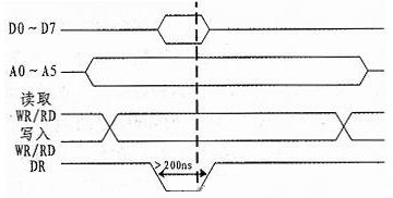
Figure 8 SbRIO read and write timing
4 Experimental results
When the ambient temperature is 25℃, the temperature rise is 80℃, the heating constant current source is set to 50 mA, the constant voltage source is set to 5 V, the on time is set to 2 300 s, and the off time is set to 7700 s. In the timing mode, the junction temperature graph is obtained by sampling every 50 ms, as shown in Figure 9. At the end, the temperature is basically difficult to reach the initial 25℃ due to the increase in the ambient temperature, but the temperature is reduced to the allowable error range. In the figure, the red line is drawn by the temperature change data measured by the sensor attached to the back of the NMOS tube, and the black line is drawn by the data calculated by the junction temperature calculation formula based on the collected data. In contrast, the change trend of the sensor measured data is consistent with the change of the calculated result data, which shows that the measurement result is accurate.
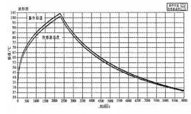
Figure 9 Temperature curve
5 Conclusion
This paper introduces a control of an aging test system on SbRIO-9612 using LabVIEW. The system achieves the predetermined acquisition data accuracy and resolution, meets the requirements of fast acquisition and fast control, and achieves good results in practical applications, with high practical value.
Keywords:LabVIEW
Reference address:Design of transistor aging test system based on LabVIEW
With the increasing requirements for the quality of electronic products in the fields of aviation, aerospace, energy industry, etc., the reliability of electronic products has received more and more attention. Electronic products will encounter different environmental conditions during use. Under the stress of thermal expansion and contraction, electronic components with poor thermal matching ability are prone to failure, resulting in electronic product failures and huge manpower and financial losses. The aging test of electronic components is to imitate or equivalent the use status of products. Through testing, non-compliant devices are eliminated, and the quality of electronic products is effectively controlled in the early stage of processing to ensure the reliability and stability of electronic products.
In view of this situation of electronic components, we have developed an aging test system that can mainly target power devices (power transistors, VDMOS, IGBT, etc.). By regularly powering on and off the components, cyclically applying electrical stress and thermal stress, and testing their ability to withstand cyclic stress.
1 Working principle
By powering on and heating the transistor, the transistor works at the current constant power. After a period of time, the junction temperature of the device continues to rise due to the heat of the transistor. After reaching the set value, the constant current source and constant voltage source are disconnected, and the device is ventilated to reduce its temperature to the set value. By repeating this process, the heating time and cooling time of the device can be calculated more accurately, achieving the purpose of intermittent testing. The basic working principle diagram is shown in Figure 1.

Figure 1 Schematic diagram of intermittent life test cycle
The thermal resistance of semiconductor devices is usually defined as:

Where RθJX = thermal resistance from device junction to specific environment (alternative symbol is θJX) [℃/W];
TJ = device junction temperature under steady-state test conditions [℃];
TX = reference temperature of the environment [℃];
PH = device power consumption [W];
The device junction temperature under test conditions can be expressed as:
Tj = TJ0 + △TJ
Where TJ0 = initial junction temperature before device heating [℃];
△TJ = device junction temperature change The
junction temperature change is expressed by temperature sensitive parameter (TSP), the formula is:
△TJ = K × △TSP
Where △TSP = temperature sensitive parameter change [mV];
K = constant defining the relationship between TJ and TSP change [℃/mV];
The temperature sensitive parameter can be expressed as:
TSP = Ie × -4Vce
Where Ie = constant current source value added at the time of cooling measurement [mV];
Vce = device junction voltage value [mV];
The K coefficient is the relationship between the junction temperature and the junction voltage. The fixed device K coefficient is a constant. The K coefficient of different devices is different. It can be found in the data of the test device or given by the manufacturer. Its calculation formula can be expressed as:

Where TJ1 and TJ2 are the junction temperatures at two moments, and Vce1 and Vce2 are the junction voltages corresponding to the junction temperatures.
2 System Architecture
The system adopts the structure of PC + sbRIO-9612 + main control board + driver board + aging board, as shown in Figure 2. The PC and 9612 communicate through the network port, and the 9612 and the main control board communicate through the digital I/O port. The power supply of sbRIO-9612, main control board, and driver board is completed by the switching regulated power supply. The programmable power supply provides working power for the devices on the aging board. The 16-channel differential AD is used to collect the current, voltage, power supply temperature and other signals of the devices to be tested on the aging board. The system uses sbRIO-9612 plus an expansion board to form a lower computer as the main control board of the system; the main control board and the driver board use bus communication. The main function of the driver board is to convert the 20 pairs of differential signals from the main control board (hardware implementation) to the driver board FPGA, and use 20 signals to communicate with sbRIO-9612. sbRIO-9612 controls the registers in the FPGA to realize the on and off of the power supply, constant current source, and drain/source, thereby establishing power circulation and appropriate sampling conditions. The hardware schematic diagram is shown in Figure 3.

Figure 2 System overall architecture diagram

Figure 3 FPGA hardware schematic diagram
The driver board and the aging board are connected by two docking sockets respectively, and the current and voltage sampling signals are transmitted back to the sbRIO-9612 board for AD conversion and then sent to the upper computer.
[page]
3 Workflow and implementation
3.1 Introduction to LabVIEW
LabVIEW is a program development environment. It uses the graphical programming language G to create source programs in the flow chart. The LabVIEW FPGA module extends the LabVIEW graphical development platform to the field programmable gate array (FPGA) on the hardware platform based on the NI reconfigurable I/O (RIO) architecture.
3.2 Workflow
At the beginning of the work, the host computer sends the control command to sbRIO-9612 according to the TCP/IP protocol. After receiving the command, according to the operation of the host computer, sbRIO-9612 sends the corresponding command and related parameters to the main control board. The main control board controls the driver board to execute the command, and then controls the aging board to perform related operations.
sbRIO-9612 is mainly composed of two parts, namely the FPGA part and the RT part; in the division of work, due to the system's requirements for speed, the fan control, programmable power supply control, temperature frequency reading, ADC acquisition, DAC transmission, differential data transmission and other modules are assigned to the fast FPGA part for execution, while the slower RT part mainly realizes the analysis of the host computer instructions, the aging work control and the data transmission from the lower computer to the upper computer. The LabVIEW FPGA workflow diagram is shown in Figure 4.

Figure 4 FPGA workflow diagram
3.3 Implementation of the working process
3.3. 1 Overview
Before the work starts, first connect to the lower computer. After the connection is successful, call the self-test module to perform self-test on the aging board to be tested. After the self-test is successful, the upper computer sends the parameters to the lower computer, and then sends the start control command. The lower computer polls the control command word of each board. After the board starts working, the heating current, measurement current, and programmable voltage required for the work are sent to the driver board through the serial data transmission module, and loaded to the corresponding aging board through the driver board. Heat the device and record the time at this time, which is the heating start time. When the difference between the current time and the heating start time is greater than or equal to the on time, stop heating, turn on the fan, record the heating end time, start AD acquisition, calculate the junction temperature based on the collected current and voltage, and send the value back to the upper computer. The upper computer draws a curve based on the temperature change. When the difference between the current time and the heating end time is greater than or equal to the off time, the cooling is completed and the measurement ends, and the next cycle is entered. After the number of cycles is reached, the board is placed in an idle state.
3.3.2 Accuracy and switching speed
1) High-speed ADC acquisition
SbRIO-9612 is integrated with AD acquisition chip. The 16-bit AD can ensure that its sampling resolution reaches 1‰. At the same time, the conversion time of 4μs ensures the sampling speed of AD. In order to eliminate the influence of common mode noise, 32 ADs are converted into 16 differential inputs. During the acquisition, 8 values are taken continuously for each channel each time to calculate the average value as the result of this acquisition. At the same time, the high-speed switch used in the aging board is used for switching to ensure the accuracy of the collected data. The following figure shows the junction voltage of the current NMOS tube (model IRFP460) and the junction temperature of the tube measured at the current moment through LabVIEW at the set measurement current of 10 mA and the programmable voltage of 12 V. The room temperature is 17.3 20 6 degrees Celsius obtained by the temperature sensor installed on each aging board. As can be seen from Figure 5, the values of the 16 channels collected by AD all begin to fluctuate after the third decimal point, ensuring that the calculated △Vf value begins to fluctuate after the second decimal point.

Figure 5 RT workflow diagram
The system can complete the acquisition of all station junction voltages within 20μs after switching from the heating state to the measurement state. In order to meet the requirements of fast acquisition, when writing the program, considering the high real-time performance of ADC, the acquisition part is assigned to the FPGA of sbRIO-9612. The Onboard Clock of sbRIO-9612 is 40 MHz, that is, a period of 0.025μs. When writing the FPGA program, the ADC acquisition configuration (that is, the switch switching command execution) and the acquisition data are placed between two adjacent frames of the sequence structure. Considering the switch switching time, a 1μs wait is added in the middle to ensure the reliability of the data, and then the data acquisition is started. The ADC acquisition part of the program is shown in Figure 6. [page]

Figure 6 AD acquisition results displayed in LabVIEW

Figure 7 ADC junction voltage acquisition program on FPGA
2) Differential data transmission
This module realizes the communication between sbRIO-9612 and FPGA. The communication mode is bus asynchronous access mode. Data is sent and received through serial DAC mode. The so-called serial DAC means that under a certain clock (clock cycle is 80 MHz), serial data is sent according to a fixed timing. First, the address is assigned to the port. The address is a total of six bits, namely A0-A5. The upper four bits are the address bits (control board number) and the lower two bits are the driver board register address; then the data is placed on the data bus. The data format is U8, set WR/RD high, then: DR is low, keep two clock cycles, DR is high, and the serial DAC writes data; similarly, when reading data, the address bus is set first, WR/RD is low, DR is low, and keep two clock cycles. The data is read within two cycles, and DR is high to complete the serial DAC read data. The entire communication module realizes the control of SbRIO-9612 to FPGA according to the communication protocol.

Figure 8 SbRIO read and write timing
4 Experimental results
When the ambient temperature is 25℃, the temperature rise is 80℃, the heating constant current source is set to 50 mA, the constant voltage source is set to 5 V, the on time is set to 2 300 s, and the off time is set to 7700 s. In the timing mode, the junction temperature graph is obtained by sampling every 50 ms, as shown in Figure 9. At the end, the temperature is basically difficult to reach the initial 25℃ due to the increase in the ambient temperature, but the temperature is reduced to the allowable error range. In the figure, the red line is drawn by the temperature change data measured by the sensor attached to the back of the NMOS tube, and the black line is drawn by the data calculated by the junction temperature calculation formula based on the collected data. In contrast, the change trend of the sensor measured data is consistent with the change of the calculated result data, which shows that the measurement result is accurate.

Figure 9 Temperature curve
5 Conclusion
This paper introduces a control of an aging test system on SbRIO-9612 using LabVIEW. The system achieves the predetermined acquisition data accuracy and resolution, meets the requirements of fast acquisition and fast control, and achieves good results in practical applications, with high practical value.
Previous article:FCT (Functional Circuit Test) Test System Based on PXI and LabVIEW
Next article:Power Quality Signal Denoising Based on LabVIEW
- Popular Resources
- Popular amplifiers
Recommended Content
Latest Test Measurement Articles
- Keysight Technologies Helps Samsung Electronics Successfully Validate FiRa® 2.0 Safe Distance Measurement Test Case
- From probes to power supplies, Tektronix is leading the way in comprehensive innovation in power electronics testing
- Seizing the Opportunities in the Chinese Application Market: NI's Challenges and Answers
- Tektronix Launches Breakthrough Power Measurement Tools to Accelerate Innovation as Global Electrification Accelerates
- Not all oscilloscopes are created equal: Why ADCs and low noise floor matter
- Enable TekHSI high-speed interface function to accelerate the remote transmission of waveform data
- How to measure the quality of soft start thyristor
- How to use a multimeter to judge whether a soft starter is good or bad
- What are the advantages and disadvantages of non-contact temperature sensors?
MoreSelected Circuit Diagrams
MorePopular Articles
- LED chemical incompatibility test to see which chemicals LEDs can be used with
- Application of ARM9 hardware coprocessor on WinCE embedded motherboard
- What are the key points for selecting rotor flowmeter?
- LM317 high power charger circuit
- A brief analysis of Embest's application and development of embedded medical devices
- Single-phase RC protection circuit
- stm32 PVD programmable voltage monitor
- Introduction and measurement of edge trigger and level trigger of 51 single chip microcomputer
- Improved design of Linux system software shell protection technology
- What to do if the ABB robot protection device stops
MoreDaily News
- Allegro MicroSystems Introduces Advanced Magnetic and Inductive Position Sensing Solutions at Electronica 2024
- Car key in the left hand, liveness detection radar in the right hand, UWB is imperative for cars!
- After a decade of rapid development, domestic CIS has entered the market
- Aegis Dagger Battery + Thor EM-i Super Hybrid, Geely New Energy has thrown out two "king bombs"
- A brief discussion on functional safety - fault, error, and failure
- In the smart car 2.0 cycle, these core industry chains are facing major opportunities!
- The United States and Japan are developing new batteries. CATL faces challenges? How should China's new energy battery industry respond?
- Murata launches high-precision 6-axis inertial sensor for automobiles
- Ford patents pre-charge alarm to help save costs and respond to emergencies
- New real-time microcontroller system from Texas Instruments enables smarter processing in automotive and industrial applications
Guess you like
- Share: MSP430F149 drives ADS1216 code
- The FD pin in the NFC chip cannot detect any events and the program enters an infinite loop. What should I do to pull the FD pin low?
- Cadence Allegro 16.6 Practical Essential Tutorial
- Regarding the reading distance of low-frequency cards
- Do you expand your application directly on the official board, or do you need to draw a new board yourself?
- DIY open source electric car color screen charger
- Looking to buy esp32-wrover-B module or development board
- IEEE754 floating point format
- EEWorld will meet you offline and give you a 2,000 yuan ticket. Please come to the lucky draw.
- What you should know about electronic circuit maintenance: resistors

 EL5166ISZ


 京公网安备 11010802033920号