AI is here, and the concept of glass substrate is too popular
Latest update time:2024-05-29
Reads:
Last week, a new concept of chip packaging went completely crazy, and related concept stocks set off a surge in daily price, which is glass substrate. Then, Intel also announced last week that it would participate in this competition, increasing orders to multiple equipment and material suppliers to seize the glass substrate packaging.
Yesterday, a piece of news added fuel to the fire for glass substrates - Absolics, a glass substrate company jointly established by SK and Applied Materials, will receive up to US$75 million in subsidies from the US Chip Act, making it the first company in the materials field to receive subsidies.
However, this fire seemed to be burning a little too fiercely.
Fu Bin | Author
Electronic Engineering World (ID: EEWorldbbs) | Produced
 Pushing the limits of chips

 Pushing the limits of chips

In a nutshell, the various characteristics of glass substrates can surpass the performance of chips, which is particularly suitable for the current situation where AI computing power is in short supply. That’s why there is a saying: “Whoever first realizes the large-scale commercialization of glass substrates will be the new game changer in the substrate industry.”
The so-called glass substrate actually refers to the packaging substrate. As the number of transistors in early large-scale integrated chips continued to increase, they needed to be connected to more pins, and packaging substrates came into being.
Since the 1970s, substrate designs have continued to evolve, including metal frames, ceramic chips, and organic packages (plastic substrates).
For more than 20 years, organic plastics have been the main material for packaging substrates, but as the number of chips and connections in a single package increases, organic substrates are approaching their physical limits.
In particular, the rough surface of organic substrates can affect the inherent performance of ultra-fine circuits. In addition, organic materials may shrink or warp during the manufacturing process, causing defects in chips.
As a result, the idea of replacing organic substrates with glass is gaining traction in the semiconductor industry. Glass substrates are better in every way: they are flatter (important for attaching flat silicon wafers to very flat motherboards), stiffer (better at accommodating more and smaller wires), and more stable.
Moreover, manufacturing the substrate with glass as the raw material allows the processing chip and the memory chip to be packaged into a single device, which is not only thinner, but also reduces energy consumption by more than 30% and processes data very quickly.
In addition to performing better at basic functions, glass substrates are expected to increase interconnect density and optical interconnect integration by 10 times, allowing future chips to process more data faster.

Performance comparison between organic material substrate and glass substrate
For 2.5D/3D packaging, glass through vias have more significant advantages than silicon through vias. This is because silicon is a semiconductor material, and the carriers around TSV can move freely under the action of electric or magnetic fields, affecting adjacent circuits or signals, and thus affecting chip performance. Glass materials have no freely moving charges, excellent dielectric properties, and CTE (coefficient of thermal expansion) is close to that of silicon. Glass through via (TGV) technology that uses glass instead of silicon can avoid TSV problems. At the same time, TGV technology does not require the production of an insulating layer, reducing process complexity and processing costs.

More importantly, the characteristics of glass substrates are very suitable for chiplets. Since the chiplet design puts forward new requirements for the signal transmission speed, power supply capacity, design and stability of the substrate, these requirements can be met after switching to glass substrates.
From this perspective, glass substrates are "full of buff points" and can be used to support any new concept. Especially when Moore's Law is slowing down, it can enhance chip performance from another perspective.
 Who is advancing glass substrates?

 Who is advancing glass substrates?

Although the concept of glass substrate seems to have been popularized by Nvidia's GB200, in fact, Intel is the pioneer of glass substrates. At the same time, Intel, AMD, and Samsung Electronics have long intended to adopt glass substrate technology, and it is estimated that it will be put into use as early as 2026.
In September 2023, Intel announced the launch of a glass substrate for the next generation of advanced packaging, which is scheduled for mass production from 2026 to 2030. According to Intel's description at the time, this innovation took more than ten years of research to perfect.
The glass substrate has “better thermal, physical and optical properties” than modern organic substrates, which can increase interconnect density by 10 times. The glass substrate can also withstand higher operating temperatures and can reduce pattern distortion by 50% through enhanced flatness, thereby increasing the focus depth of lithography and giving designers more flexibility in power delivery and signal routing.
For decades, Intel has also been the "leader in the semiconductor industry." In the 1990s, Intel took the lead in the transition from ceramic packaging to organic packaging and was the first to introduce halogen-free and lead-free packaging.
Samsung, a strong rival of Intel in the packaging field, has also deployed this technology.
Samsung Electro-Mechanics officially entered the semiconductor glass substrate market at CES 2024 in January this year, and announced a roadmap to build a pilot line this year, mass-produce prototypes next year, and mass-produce in 2026. Then in early May, it was confirmed that the introduction of semiconductor glass substrate pilot line equipment will be completed in September.
At present, the main equipment partners for the pilot line construction include Philoptics, Chemtronics, Joongwoo M-Tech, Germany's LPKF, etc.
In addition, some Japanese and Korean companies have also announced their entry into the glass substrate business. For example, SK and chip equipment giant Applied Materials have jointly established Absolics, which has begun small-scale mass production and may plan to start mass production this year; in March this year, LG Innotek, a subsidiary of LG invested by Apple, announced its entry into the semiconductor glass substrate business; Japan's Dai Nippon Printing (DNP) demonstrated a new development in semiconductor packaging, the Glass Core Substrate (GCS), which is said to solve many problems caused by ABF and is ready for mass production in 2027; in October last year, it announced that it plans to develop glass substrates as a new business.
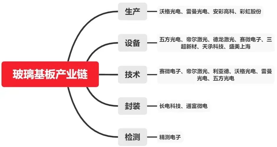
The glass substrate itself involves an ecosystem of multiple key links, including production, equipment, technology, packaging and testing. Each part is indispensable, especially PCB and substrate. Therefore, companies such as Corning in the United States, Shentai in the United States, Tecnologia and KISO WAVE in Japan will be key to the development of glass substrates.
From this, it is not difficult to see that the road to glass substrates is never a one-man show, but requires a huge industrial chain.
 Glass substrate, too much?

 Glass substrate, too much?

Although the concept is hot, a large-scale explosion is still some distance away. Technical development is not easy, and the same is true for replacing organic substrates with glass substrates.
Other challenges include figuring out what kind of glass is most effective; how to layer metals and devices to add microvias and routing; and once the device is assembled, how to better dissipate heat and withstand mechanical forces throughout the product’s lifecycle.
There are more practical problems: how to make the edges of glass less likely to crack; how to split large glass substrates; and how to protect glass substrates from bouncing off conveyor belts or rollers or flying off when transported within the factory.
So we can see that both Intel, which has been researching for ten years, and Japanese and Korean companies have given a time period of 2026. Only Absolics is expected to start production in the second and fourth quarters of this year.
The industry generally agrees that prototype production will begin in 2025, with full-scale production set to begin in 2026.
According to Prismark statistics, the global IC packaging substrate industry is expected to reach US$21.4 billion in 2026. With the entry of major chip giants, the replacement of glass substrates for silicon substrates will accelerate, and the penetration rate of glass substrates is expected to reach 30% within 3 years and more than 50% within 5 years.
According to Morgan Stanley's previous forecast, there is a certain time difference with the above time period: Nvidia's GB200 DGX/MGX supply chain has been launched, and GB200 will use glass substrates for advanced packaging. GB200 chips are expected to deliver about 420,000 to the market in the second half of 2024, and production is expected to be about 1.5 million to 2 million by 2025.
TSMC has not yet announced any technology related to glass substrates, so whether GB200 can catch up with glass substrates depends on the speed of Absolics.
The speed of concept speculation is always faster than the technology itself. The domestic related industry chain companies that have become popular this time include Voger Optoelectronics, Leman Optoelectronics, Ancai Hi-Tech, Rainbow Holdings, Wufang Optoelectronics, Delong Laser, Saiwei Electronics, Sanchao New Materials, Tiancheng Technology, Shengmei Shanghai, Saiwei Electronics, Delong Laser, Leyard, Voger Optoelectronics, Leman Optoelectronics, Wufang Optoelectronics, Changdian Technology, Tongfu Microelectronics, and Jingce Electronics.

In short, it will take at least one or two years for glass substrates to be truly commercialized. Don't be emotional about this new technology in the short term, but take a
long-term
view of it. Just like another technology in the packaging field, chiplets, they are all important, but they are definitely not something that can be accomplished by one or two players in a day or two. At the same time, before solving the packaging problem, there are other problems to be solved first.
references
· END ·


 京公网安备 11010802033920号