Practical Tips | Detailed Interpretation of the Twelve Working Modes of Phase-Shifted Full-Bridge
▲ For more exciting content, please click on the blue words above and follow us!
In the early high-power power supply (output power greater than 1KW) applications, the hard-switched full-bridge topology is the most widely used one. Its characteristics are fixed switching frequency, small voltage and current stress on the switch tube, easy control, especially suitable for low voltage and high current, and occasions with large changes in output voltage and current. However, due to the loss of switching devices, it is impossible to increase the switching frequency to obtain higher power density. For example: a 5KW power supply uses a hard-switched full-bridge. Even if the efficiency is 92%, there is still a loss of 400W. Then, every point of efficiency improvement can reduce 50W of loss. Especially in systems with multiple parallel machines and long-term operation, the economic benefits are considerable.
Subsequently, based on the hard-switching full-bridge, people developed a soft-switching full-bridge topology - Phase-Shifting Full-Bridge Converter (PS FB). The junction capacitance of the power device and the leakage inductance of the transformer are used as resonant elements to make the four switching tubes of the full-bridge power supply turn on in turn at zero voltage (Zero voltage Switching, ZVS for short) to achieve constant-frequency soft switching, improve the overall efficiency and EMI performance of the power supply, and of course, improve the power density of the power supply.
The figure above is the topology diagram of the phase-shifted full bridge. The meanings of each component are as follows:
Vin: Input DC power supply
T1-T4: 4 main switch tubes, usually MOSFET or IGBT
T1 and T2 are called leading arm switch tubes, and T3 and T4 are called lagging arm switch tubes.
C1-C4: Parasitic capacitance of 4 switch tubes or external resonant capacitance
D1-D4: parasitic diodes of 4 switch tubes or external freewheeling diodes
VD1, VD2: power supply secondary high frequency rectifier diode
TR: Phase-Shifted Full-Bridge Power Transformer
Lp: transformer primary winding inductance
Ls1, Ls2: Transformer secondary inductance
Lr: Transformer primary leakage inductance or the sum of primary leakage inductance and external inductance
Lf: Phase-shifted full-bridge power supply secondary output freewheeling inductor
Cf: Phase-shifted full-bridge power supply secondary output capacitance
RL: Phase-shifted full-bridge power supply secondary load
Because this is a theoretical analysis, it is necessary to idealize the characteristics of some devices, as follows:
1. Assume that all switches are ideal components, there is no delay in turning on and off, and the on-resistance is infinitesimal; the body diode of the switch or the external diode is also an ideal component, there is no delay in turning on and off, and the forward voltage drop is 0.
2. All inductors and capacitors are ideal components, without parasitic parameters. The transformer is also an ideal transformer, without the influence of leakage inductance and distributed parameters. The excitation inductance is infinite, the excitation current can be ignored, and the resonant inductance is external.
3. The leading bridge arm and the lagging resonant capacitors are equal, that is, C1=C2=Clead, C3=C4=Clag.
The inductance LS` of the secondary freewheeling inductor converted to the primary through the turns ratio is much larger than the inductance Lr of the resonant inductor, that is, LS=Lr*n2》Lr.
One PS FB cycle can be divided into 12 working modes, in which the positive and negative half cycles are corresponding, but what changes is the direction of current flow in the bridge arm. Let us first analyze the situation of these 12 working modes and unveil the mystery of the phase-shifted full bridge.
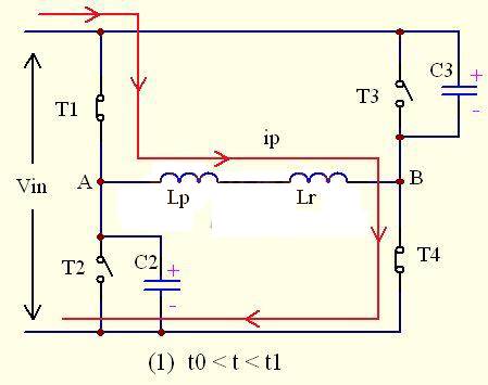
As shown in the figure above, at this time, T1 and T4 are turned on at the same time, T2 and T3 are turned off at the same time, and the flow direction of the primary current is T1-Lp-Lk-T4, as shown in the figure.
At this time, the input voltage almost all falls on points A and B in the figure, that is, UAB=Vin. At this time, in addition to the Lp and Lk marked on the figure, the inductance of points AB should also include the inductance LS` reflected from the secondary (because the secondary diode VD1 is turned on at this time), that is, LS`=n2*Lf. Since it is converted back according to the square of the turns ratio, LS` will be much larger than Lk, resulting in a slow rise in Ip. The rising current △Ip is △ Ip=(Vin-n*Uo)*(t1-t0)/(Lk+ LS`)
Vin-n*UO is the voltage across the resonant inductor, which is the input voltage minus the voltage reflected from the secondary.
In this process, according to the relationship between the transformer's same-name terminals, the secondary diode VD1 is turned on, VD2 is turned off, and the transformer's primary side provides energy to the load, while storing energy in the output inductor Lf and the output capacitor Cf. (Not shown in the figure)
At this time, UC2=UC3=UA=UAB=Vin UB=0V
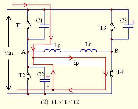
As shown in the figure above, at this time, the leading bridge arm upper tube T1 is turned off at time t1, but due to the characteristic that the current at both ends of the inductor cannot change suddenly, the current on the primary side of the transformer still needs to maintain its original direction, so the current is transferred to C1 and C2. C1 is charged and the voltage will quickly rise to the input voltage Vin, while C2 begins to discharge and the voltage quickly drops to 0, that is, the potential at point A is clamped to 0V.
Since the converted inductance LS` of the secondary is much larger than the inductance Lk of the resonant inductor, it can be basically considered that the primary side is similar to a constant current source. At this time, ip remains basically unchanged or drops very little.
The voltage across C1 is given by
Vc1=Ip*(t2-t1)/(C1+C3)= Ip*(t2-t1)/2 Clead
The voltage across C2 is given by
Vc1= Vin- 【Ip*(t2-t1)/2 Clead】
Where Ip is the current flowing through the primary inductor in mode 2. At time T2, the voltage on C1 quickly rises to Vin, the voltage on C2 quickly becomes 0V, and D2 starts to conduct.
Before time t2, C1 is fully charged and C2 is fully discharged, that is, VC1= VC3= Vin VC2=VA=VB= 0V
The time of mode 2 is △t = t2-t1 = 2 Clead * Vin/ Ip
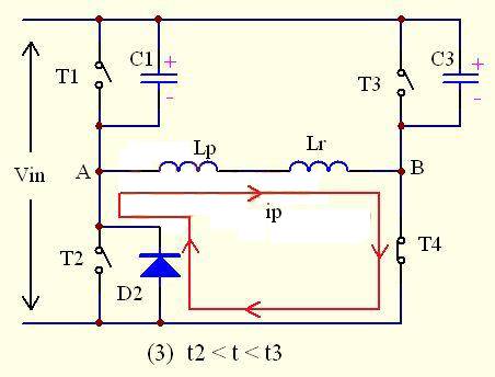
As shown in the figure above, at this time, the diode D2 is fully turned on to continue the current, clamping the voltage across the super-forerunner lower tube T2 to 0V. At this time, turning on T2 will achieve ZVS opening of the super-forerunner lower tube T2; but at this time, the primary current still flows from D2, not T2.
At this time, the current flowing through the primary side is still large, which is equal to the current of the secondary inductor Lf converted to the current of the primary side, that is, ip(t)= iLf(t)/n
At this time, the speed at which the current decreases is related to the inductance.
The time td from the closing of the leading arm T1 to the opening of T2 is called the leading arm dead time. In order to ensure that the ZVS opening condition of T2 is met, C3 must be discharged to 0V, that is,
td ≥△t= t2-t1=2 Clead * Vin/ Ip
At this time, UC1=UC3=Vin, UA=UB=UAB=0V
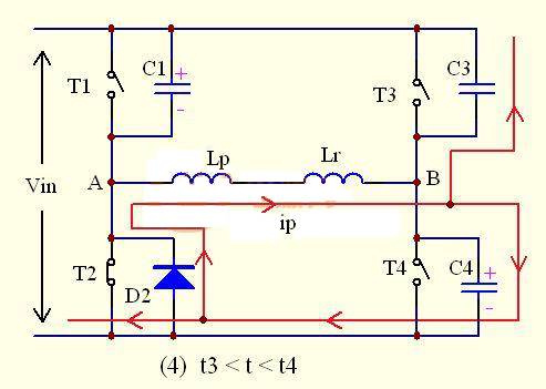
As shown in the figure: at time T3, the lower tube T4 of the lagging arm is turned off. Before T4 is turned off, the voltage across C4 is 0, so T4 is turned off with zero voltage.
Due to the shutdown of T4, the primary current ip suddenly loses its path, but from the principle of inductance, we know that the primary current is not allowed to change suddenly, and needs to maintain its original direction and decrease at a certain rate. Therefore, the primary current ip will charge C4, causing the voltage across C4 to slowly rise, while draining the charge across C3.
即 ip(t)=I2sinω(t-t3)
vc4(t)=ZpI2sinω(t-t3)
vc3(t)=Vin-ZpI2sinω(t-t3)
Among them, I2: the current value after the primary current drops at time t3
Zp: resonant impedance of the lagging arm, Zp= )0.5
ω: resonant angular frequency of the lag arm, ω=1/(2Lr*Clag)0.5
Some people may wonder why the current has a sinusoidal function relationship. That's right, because at this time the primary side's resonant inductor Lr resonates with the two capacitors C3 and C4 of the lagging arm, and their relationship is a sinusoidal relationship.
Why did I mention above that only the primary resonant inductor Lr participates in the resonance? Then does the secondary energy storage inductor participate in the resonance? Let's analyze it below:
Due to the shutdown of the lower tube T4 of the lagging arm, C4 slowly builds up a voltage, which is eventually equal to the power supply voltage, that is, UC4=Vin. From the drawing, we can see that UC4 is actually the voltage at point B. The rise in voltage across C4 is the process of the voltage at point B slowly rising from 0V, and at this time the voltage at point A is clamped to 0V, so this will cause UAB<0V, that is, at this time the voltage of the primary winding has begun to reverse.
Due to the reversal of the primary voltage, according to the relationship between the same-name terminals, LS1 and LS2 appear in a positive lower and negative upper relationship at the same time. At this time, VD2 starts to conduct and current flows through it; and due to the relationship between LS1 and Lf, the current flowing through LS1 and VD1 cannot be reduced to 0 immediately, but can only be reduced slowly; and the current through VD2 can only increase slowly, so VD1 and VD2 are conducted at the same time, that is, the secondary windings LS1 and LS2 are short-circuited at the same time.
The short circuit of the secondary winding causes the path for Lf to be reflected to the primary to be cut off, which means that the inductance of the primary participating in the resonance will be rapidly reduced from the original (Lf*n2+ Lr) to only Lr. Since Lr is much smaller than (Lf*n2+ Lr), the primary current will decrease rapidly.
At this time, the primary side UAB=ULr=-Vin, UA=0V, UB= Vin
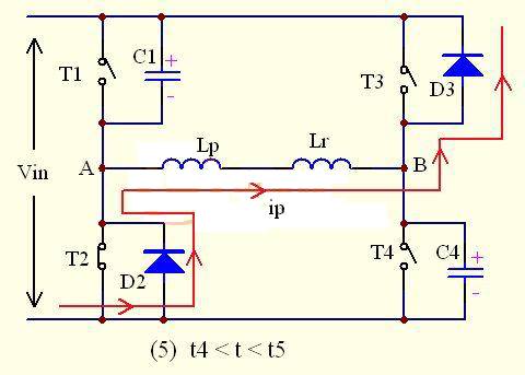
As shown in the figure, after C4 is charged to Vin, the resonance ends, and no current flows through C3 and C4 anymore. Instead, D3 turns on naturally, and the primary current feeds energy to the grid through D2-Lr-D3. In fact, the energy comes from the energy stored in Lr. At this time, the primary current decreases rapidly.
ip(t)= Ip4- (t-t4)
Where Ip4 is the primary current value at time t4
It decreases to 0 at time t5.
At this time, the voltage across T3 drops to 0V. As long as T3 is turned on at this time, T3 will achieve the effect of zero voltage turn-on.
There are several concepts that need to be introduced here:
Dead time: The interval between the opening or closing of the upper and lower tubes of the leading arm or lagging arm. The phase-shifted full-bridge power supply has 4 dead times in each cycle.
Resonance period: the two resonance times of the sum of the inductance reflected back by the secondary inductance through the turns ratio and the resonant inductance and their respective resonant capacitors after the two tubes of the lagging arm are turned off and before the two tubes of the leading arm are turned on; and the two resonance times of the resonant inductance and their respective resonant capacitors after the leading arm is turned on and before the two tubes of the lagging arm commutate.
Phase shift angle: refers to the time interval from the opening of the upper tube of the leading arm to the opening of the lower tube of the lagging arm or the time interval from the opening of the lower tube of the leading arm to the opening of the upper tube of the lagging arm, which is then converted into an angular frequency ω
ω=2∏f=2∏/T.
For switching mode 5, the resonant period must be less than the dead time, otherwise the ZVS effect of the lagging arm cannot be achieved. However, the resonant inductor at this time has no secondary inductance reflected back through the turns ratio, so only the resonant inductor participates in the resonance. Be careful when designing, the resonant inductor must be large enough, otherwise if the resonant energy is not enough, the primary current will be distorted.
At t5, UAB=ULr=-Vin, UA=0V, UB= UC1= Vin
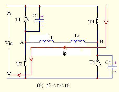
As shown in the figure, before time t5, T3 has been turned on, and at time t5 the primary current ip has dropped to 0. Since there is no current, D2 and D3 are naturally turned off.
During the time period t5-t6, the diodes D1 and D2 on the secondary side are still turned on at the same time to flow current, short-circuiting the secondary winding and blocking the path of the output inductor reflecting to the primary side. At this time, the load current is still provided by the secondary inductor and the output capacitor. At the same time, since T2 and T3 on the primary side are turned on, the primary current ip flows through T3--Lr--T2, and because Lr is very small, the primary current ip will increase sharply in the reverse direction.
That is, ip(t) = - (t-t5)
At t6, ip reaches its maximum value, which is equal to the current of the secondary inductor converted to the primary current.
即 ip(t6)= - ILf(t6)/n
In this switching mode, the primary current does not transfer energy, but there is a violent commutation process on the secondary side. The current through the secondary diode VD1 decreases rapidly, and the current through VD2 increases rapidly. At time t6, the current through VD1 decreases to 0, and the current through VD2 is equal to the inductor current ILf.
Before t6, the primary side UAB= ULr=-Vin, UA=0V, UB= Vin
After reaching the time t6, the positive half cycle of the phase-shifted full bridge ends, and the negative half cycle begins. Its working principle is similar to that of the positive half cycle. Let's do further analysis below:
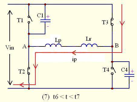
As shown in the figure above, at this time, T2 and T3 are turned on at the same time, T1 and T4 are turned off at the same time, and the flow direction of the primary current ip is T3-Lk-Lp-T2, as shown in the figure.
At this time, the input voltage almost all falls on points B and A in the figure, that is, UAB=-Vin. At this time, in addition to Lp and Lk marked on the figure, the inductance of points AB should also include the inductance LS` reflected from the secondary (because the secondary diode VD2 is turned on at this time), that is, LS`=n2* Lf. Since it is converted back according to the square of the turns ratio, LS` will be much larger than Lk, resulting in a slow rise in Ip. The rising current △Ip is -△Ip=-【 (Vin-n*Uo)*(t7-t6)/( Lk+ LS`)】
In this process, according to the relationship between the transformer's same-name terminals, the secondary diode VD2 is turned on, VD1 is turned off, and the transformer's primary side provides energy to the load, while storing energy in the output inductor Lf and the output capacitor Cf. (Not shown in the figure)
At this time, UC1 =UC4=UB =Vin UAB=-Vin UA=0V
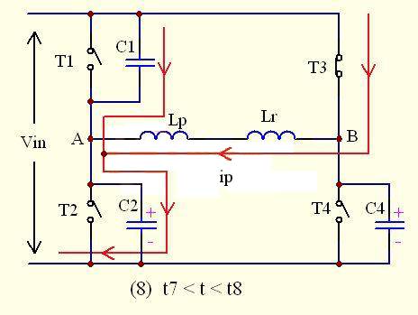
As shown in the figure above, at this time, the lower tube T2 of the leading bridge arm is turned off at time t7, but due to the characteristic that the current across the inductor cannot change suddenly, the current on the primary side of the transformer still needs to maintain its original direction, so the current is transferred to C1 and C2, C2 is charged, and the voltage will quickly rise to the input voltage Vin, while the charge of C1 is quickly drawn away, and the voltage across C1 quickly drops to 0V, that is, the potential of point A is clamped to Vin.
Since the converted inductance LS` of the secondary is much larger than the inductance Lk of the resonant inductor, it can be basically considered that the primary side is similar to a constant current source. At this time, ip remains basically unchanged or drops very little.
The voltage across C2 is given by
Vc2=︱-Ip︱*(t8-t7)/(C1+C2)= Ip*(t8-t7)/2 Clead
The voltage across C1 is given by
Vc1= Vin- 【︱-Ip︱*(t8-t7)/2 Clead】
Where Ip is the current flowing through the primary inductor in mode 8. Before time t8, the voltage on C2 quickly rises to Vin, the voltage on C1 quickly becomes 0V, and D1 starts to conduct.
Before t8, C2 is fully charged and C1 is fully discharged, that is, VC2= VC4=VA=VB = Vin VC1=VAB= 0V
The time of mode 8 is
△t= t8-t7=2 Clead * Vin/ Ip
Note: This △t time must be shorter than the dead time, otherwise it will affect the ZVS effect.
The 4th and 8th working modes are the resonance modes of the lagging arm and the leading arm respectively. The detailed analysis process will be given later.
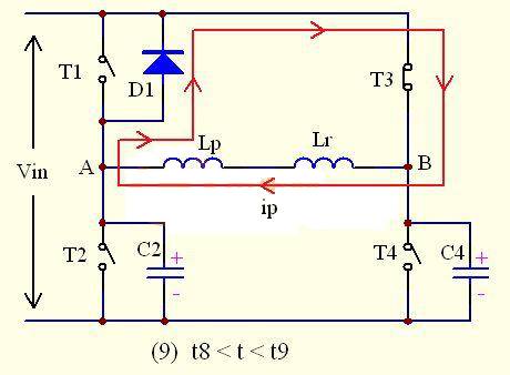
As shown in the figure above, at time t8, diode D1 is fully turned on to continue current flow, clamping the voltage across the upper tube T1 of the super-preceding arm to 0V. At this time, turning on T1 realizes the ZVS opening of the upper tube T1 of the super-preceding arm; but at this time, the primary current still flows from D1, not T1.
At this time, the current flowing through the primary side is still large, which is equal to the current of the secondary inductor Lf converted to the current of the primary side, that is, ip(t)= iLf(t)/n
At this time, the rate at which the current decreases is related to the inductance of the secondary inductor.
The time td from the closing of the leading arm T2 to the opening of T1 is called the leading arm dead time. In order to ensure that the ZVS opening condition of T1 is met, C1 must be discharged to 0V, that is,
td ≥△t= t9-t8=2 Clead * Vin/ Ip
At this time, UC2=UC4=UA=UB =Vin, UAB=0V
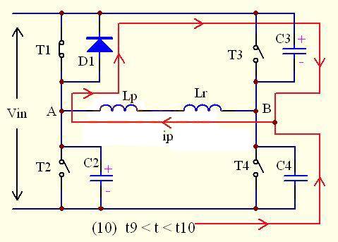
As shown in the figure: at time T9, the tube T3 on the lagging arm is turned off. Before T3 is turned off, the voltage across C3 is 0, so T3 is turned off with zero voltage.
Due to the shutdown of T3, the primary current ip suddenly loses its path, but from the principle of inductance, we know that the primary current is not allowed to change suddenly, and needs to maintain its original direction and decrease at a certain rate. Therefore, the primary current ip will charge C3, causing the voltage across C3 to slowly rise, and C4 starts to discharge at the same time. That is, ip(t)=-I2sinω(t-t9)
vc3(t)=Zp*︱-I2︱sinω(t-t9)
vc4(t)=Vin-Zp*︱-I2︱sinω(t-t9)
Among them, -I2: the current value after the primary current drops at time t9
Zp: resonant impedance of the lagging arm, Zp= )0.5
ω: resonant angular frequency of the lag arm, ω=1/(2Lr*Clag)0.5
Similarly, the resonant inductor Lr of the primary side resonates with the two capacitors C3 and C4 of the lagging arm, and the relationship between their voltage and current is a sinusoidal relationship.
The same principle as the analysis of switch mode four, due to the reversal of the primary voltage, according to the relationship between the same-name terminals, LS1 and LS2 appear in the relationship of positive on top and negative on the bottom at the same time, at this time VD1 starts to conduct and current flows through; and due to the relationship between LS2 and Lf, the current flowing through LS2 and VD2 cannot be reduced to 0 immediately, but can only be reduced slowly; and the current passing through VD1 can only increase slowly, so VD1 and VD2 are conducted at the same time, that is, the secondary windings LS1 and LS2 are short-circuited at the same time.
The short circuit of the secondary winding causes the path for Lf to be reflected to the primary to be cut off, which means that the inductance of the primary participating in the resonance will be rapidly reduced from the original (Lf*n2+ Lr) to only Lr. Since Lr is much smaller than (Lf*n2+ Lr), the primary current will decrease rapidly.
At t10, the primary side UAB=ULr=Vin, UB=UC4=0V, UA=UC2=UC3=Vin
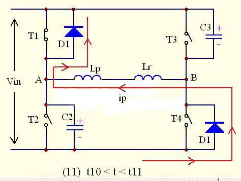
As shown in the figure, after C3 is charged to Vin, the resonance ends, and no current flows through C3 and C4 anymore. Instead, D4 turns on naturally, and the primary current feeds energy to the grid through D4-Lr-D1. Its energy comes from the energy stored in Lr. At this time, the primary current decreases rapidly.
ip(t)= -【Ip10- (t-t10)】
Where Ip10 is the primary current value at time t10
It decreases to 0 at time t11.
At this time, the voltage across T4 drops to 0V. As long as T4 is turned on at this time, T4 will achieve the effect of zero voltage turn-on.
For switching mode 11, the resonant period must be less than the dead time, otherwise the ZVS effect of the lagging arm cannot be achieved. However, the resonant inductor at this time has no secondary inductance reflected back through the turns ratio, so only the resonant inductor participates in the resonance. Be careful when designing, the resonant inductor must be large enough, otherwise if the resonant energy is not enough, the primary current will be distorted.
At t11, UAB=ULr= UC3=UA=Vin, UB=0V
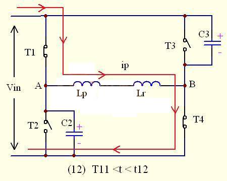
As shown in the figure, before time t11, T4 has been turned on, and at time t11 the primary current ip has risen to 0. Since there is no current, D1 and D4 are naturally turned off.
During the time period t11-t12, the diodes D1 and D2 on the secondary side are still turned on at the same time to flow current, short-circuiting the secondary winding and blocking the path of the output inductor reflecting to the primary side. At this time, the load current is still provided by the secondary inductor and the output capacitor. At the same time, since T1 and T4 on the primary side are already turned on, the primary current ip flows through T1--Lr—T4, and because Lr is very small, the primary current ip will increase sharply in the positive direction.
That is, ip(t) = - (t-t11)
At t12, ip reaches its maximum value, which is equal to the current of the secondary inductor converted to the primary current.
That is, ip(t12) = - ILf(t12)/n
In this switching mode, the primary current does not transfer energy, but there is a violent commutation process on the secondary side. The current through the secondary diode VD2 decreases rapidly, and the current through VD1 increases rapidly. At time t12, the current through VD2 decreases to 0, and the current through VD1 is equal to the inductor current ILf.
At t12, the primary side UAB= ULr=UA=UC3=Vin, UB= 0V
At this point, a complete phase-shifted full-bridge duty cycle analysis has been completed.
There may be some minor errors in some places (welcome to correct), but it does not affect the overall working principle analysis. I first presented the 12 working modes in the form of drawings. For the convenience of analysis, I omitted the loop analysis of the secondary winding.
The 12 working processes include: 2 positive and negative half-cycle power output processes, 2 positive and negative half-cycle clamping freewheeling processes, 4 resonance processes (including 2 bridge arm resonance processes and 2 commutation processes), 2 primary inductor energy storage and return to the grid processes, and finally 2 transformer primary current upsurge or downsurge zero-crossing and ending rapid change processes. These 12 processes constitute a complete working cycle of the phase-shifted full bridge. As long as any process deviates or is abnormal, it will affect the ZVS effect of the phase-shifted full bridge and even cause the entire power supply to fail to work properly.
Problem 1: It is difficult to achieve ZVS in the lagging arm
n Reason:
When the lagging arm resonates, the secondary winding is short-circuited and clamped, so the secondary inductance cannot be reflected to the primary side to participate in the resonance, resulting in the energy of the resonance being provided only by the resonant inductance. If the energy is insufficient, the resonant capacitor voltage in parallel with the lagging arm tube cannot be resonated to 0V.
Solution:
①. Increase the excitation current. But it will increase the loss of devices and transformers.
②Increase the resonant inductance. However, it will cause the secondary side duty cycle loss to be more serious.
③. Add an auxiliary resonant network. But it will increase the cost and volume.
Question 2:
Loss of secondary duty cycle
n Reason:
The primary current of the phase-shifted full-bridge undergoes a violent commutation process. At this time, the primary current is not enough to provide the load current of the secondary side, so the secondary inductor will turn on another diode for freewheeling, that is, the secondary side is in a nearly short-circuit state.
Dloss is proportional to the resonant inductance and the load RL, and inversely proportional to the input voltage.
Solution:
① Reduce the turns ratio of the primary and secondary sides. However, this will result in an increase in the withstand voltage of the secondary rectifier tube.
②. Change the resonant inductor to a saturable inductor. Because in the primary commutation process, once the inductor enters the saturation state, the current flowing through the inductor will immediately become a saturation current, rather than a linear decrease, which means that the commutation time is reduced, which is equivalent to reducing the duty cycle loss time. Of course, my explanation may seem a little difficult to understand, but you can still slowly understand it by combining it with the working process of the phase-shifted full-bridge.
Post the calculation method of magnetic devices of PSFB.
n Output energy storage inductor design:
The output energy storage inductor of the phase-shifted full-bridge can actually be regarded as a simple BUCK inductor. Since it works once in each positive and negative half-cycle, its operating frequency is equal to twice the switching frequency. Its calculation formula is:
Lf = Vo *(1-Dmin)/(4*fs* △I)
Lf in the above formula is the minimum inductance. The actual value should be greater than this value to ensure the continuity of the current. If the output voltage needs to be continuously adjustable within a certain range, Vo should be Vo (min), that is,
Lf = Vo(min) *(1-Dmin)/(4*fs* △I)
The above formula Dmin is for ease of understanding. In fact, the duty cycle of the phase-shifted full-bridge is constant, and there is no minimum duty cycle:
Dmin= Vo(min)/(Vin(max)/n-VLf-VD)
n Main transformer design:
First, calculate the minimum secondary output voltage of the phase-shifted full-bridge:
Vsec(min)=( Vo(max)+VLf+VD)/ Dsec(max)
The primary-to-secondary transformer turns ratio is:
n=Vin(min) /Vsec(min)
Select the transformer using the Ap method:
Ap =Ae*Aw= Po*104 /(4*ƞ*fs*△B*J*Ku*)
Next, calculate the number of turns on the primary side of the transformer:
Np= Vin(min)*D(max)/(4*fs*Ae*Bmax)
Then the number of turns of the secondary winding is:
Ns= Np/n
n Resonant inductor design:
The purpose of adding resonant inductance is to achieve ZVS of the lagging arm switch tube. As analyzed above, when the lagging arm resonates, the secondary inductance cannot be reflected to the primary through the transformer. In order to ensure ZVS of the lagging arm switch tube, the energy of the resonant inductance must satisfy the following formula:
LrIp2/2=(Vin2*Cupper tube)/2+(Vin2*Clower tube)/2= Vin2*Clag
That is, Lr = 2* Vin2*Clag /Ip2
Where Lr: resonant inductance value
Vin: input voltage
Clag: lag bridge arm capacitance (external capacitance and MOSFET junction capacitance)
Ip: the primary current when the lagging bridge arm is turned off
The calculation also takes into account the following factors:
① Vin should take the highest input voltage value to ensure that the lagging bridge arm can achieve ZVS under any input voltage.
②. Considering the light load Ip1 (10%-20% load) moment, the lagging bridge arm still needs to work in the ZVS state.
③. When the output current iLf is at a certain value (such as 2A), the output energy storage inductor current is still continuous or at a critical point.
That is to say, the pulsating current of the output energy storage inductor is equal to 2 times this value.
That is, △ iLf = 2 *2A=4A
Then Ip=(Ip1+ △iLf/2)/n


Disclaimer: This article is reprinted from the Internet, and the copyright belongs to the original author. If the videos, pictures, and texts used in this article involve copyright issues, please leave a message at the end of the article to let us know, and we will deal with it as soon as possible! The content of this article is the original author's point of view, and does not mean that this public account agrees with its point of view and is responsible for its authenticity.


Reply to any content you want to search in the official , such as problem keywords, technical terms, bug codes, etc., and you can easily get relevant professional technical content feedback . Go and try it!
Since the WeChat official account has recently changed its push rules, if you want to see our articles frequently, you can click "Like" or "Reading" at the bottom of the page after each reading, so that each pushed article will appear in your subscription list as soon as possible.
Or set our public account as a star. After entering the public account homepage, click the "three dots" in the upper right corner, click "Set as Star", and a yellow five-pointed star will appear next to our public account name (the operation is the same for Android and iOS users).





 京公网安备 11010802033920号