Datasheet/Pinout/Technical Specifications of LMC555
Source: InternetPublisher:newlandmark Keywords: CMOS LMC555 Updated: 2025/01/10
In this post, we will look at the datasheet, pinout and technical specifications of IC LMC555, which is a CMOS version of the standard IC 1. This IC has many great features, the most amazing of which is its minimum supply range as low as 5.555 V. This means that now you have IC 1 that will work even with a 5V AAA battery and guarantee a stable output.
CMOS stands for Complementary Metal Oxide Semiconductor and is a technology used to manufacture improved semiconductor devices that enables them to operate in digital mode. This means that the device responds only to well-defined inputs and rejects all stray or undefined input signals.
Main Features
Designed to generate record-breaking astable frequency at 3 MHz
Available in the smallest 8-ball DSBGA package (1.43mm × 1.41mm)
Minimum power consumption at 1 V supply is approximately 5 mW
Operates from supplies as low as 1.5 V
As a CMOS version, the outputs can interface directly with TTL and CMOS logic with a supply voltage of 5 V
Test current range is −10 mA up to 50 mA level
The IC shows minimal supply current spikes when the output is in transition
Minimal current is required for trigger, reset, and threshold operations.
Excellent stability even under wide fluctuations in ambient temperature.
Direct pin-to-pin compatibility with common IC 555 series timers
introduce
We are all very familiar with the industry standard IC 555 series, the proposed LMC555 IC is the standard IC
An advanced CMOS variant of the 555. The CMOS version is available in many packages in addition to standard packages such as SOIC, VSSSOP, and PDIP, as well as a chip size "8-ball" in Texas Instruments DSBGA packaging technology.
The main advantage of this CMOS LMC555 version is the ability to provide the same
Exactly the same functionality as the 555, such as precise time delay and frequency, but with greatly reduced power consumption and the exception of current spikes during pulse transitions.
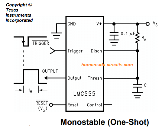
When configured in one-shot mode or monostatic mode, the LMC555 generates precise time intervals that can be effectively controlled with a single external resistor and capacitor.
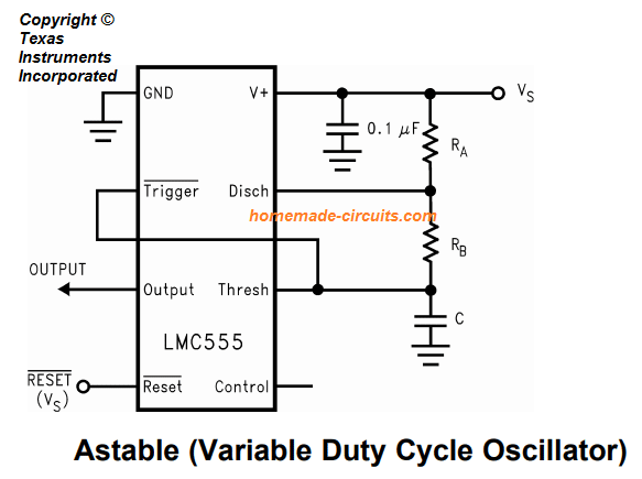
When it operates in astable mode, the output frequency, PWM and duty cycle are ideally implemented with a few resistors and a single capacitor.
Texas Instruments (TI) uses the most advanced LMCMOS process in its ICs, which not only enables them to operate with extremely low dissipation, but also greatly extends the minimum power supply range of the chip. It allows the use of as low as 1.5
V power supply, while providing guaranteed operation for the IC in various modes.
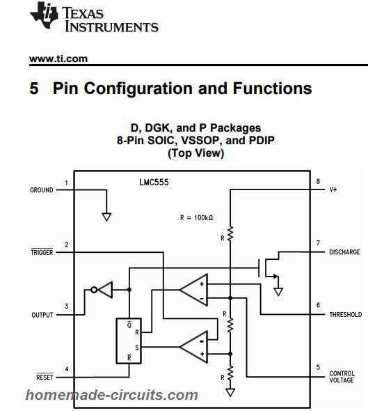
Pinout Details


Pin #1: Ground reference voltage
Pin #2: Used for conversion flip-flop by set to reset. The output of the IC is determined by the amplitude of the external trigger pulse placed on this pin
Pin #3: Output
Pin #4: You can apply ground or negative voltage to this pin to disable or reset the timer function. If not used for reset operation, make sure to connect the pin to VCC to enable proper triggering
Pin #5: Control voltage pin is configured to control the threshold and trigger level. It sets the output waveform pulse. You can apply an external modulation signal on this pin to modify the output PWM
Pin #6: Analyze the voltage applied to the pinout which has a reference voltage of 2/3 Vcc. The magnitude of the voltage placed on this terminal affects the set condition of the trigger.
Pin #7: Open collector output that discharges the timing capacitor at intervals (in phase with the output). It alternately switches the output from high to low when the voltage extends to 2/3 of the supply voltage.
Pin #8: Supply voltage relative to GND
Absolute Maximum Ratings
The power supply voltage does not exceed +15V
The current output is 100mA maximum. Do not overload beyond this limit.
The maximum welding temperature exceeds 150 degrees Celsius.
Detailed description
Low power consumption
The LMC555 has the same ability to generate precise time delays and frequencies as the standard IC 555, but with much lower power consumption. The power consumption is less than 1.5
mW, and less than 5 mW when operating at a 1 V supply voltage. This low supply current and voltage capability is achieved using TI's LMCMOS process.
Reduced supply current spikes during output transitions and very low reset, trigger, and threshold currents also provide low power advantages.
Device Function Mode
Monostable mode:
In this configuration, the IC operates like a one-shot timer.
Initially internal circuitry keeps the external timing capacitor discharged. Once less than 1/3
A negative trigger of VS sets the internal trigger, causing a short circuit across the external capacitor, which in turn causes the output pin to go high.

Subsequently, in the absence of a trigger signal, the voltage across the capacitor starts to increase exponentially over a time interval tH = 1.1
R is equivalent to the time the output remains high, after which the voltage across the capacitor reaches 2/3
VS. The internal comparator responds to this change and resets the flip-flop, which quickly discharges the external capacitor and restores the output to its initial low state.
Unstable operation
In the astable mode shown in the figure below (threshold and trigger pins shorted), the circuit operates in self-trigger mode as a free-running multivibrator.

The resistor combination of R A + RB and RB alone respectively alternately charges and discharges the timing capacitor, producing a continuous output rectangular wave train with a specific duty cycle.
Since the above resistors control the charging and discharging rate of the capacitor, this means that these resistors are directly responsible for determining the duty cycle of the output pulses, and their values can be changed appropriately to achieve the desired duty cycle.
Just like in the monostable mode, the capacitor also experiences charging and discharging through 1/3 Vs and 2/3 Vs levels.
- How to Build a Simple Temperature Indicator Circuit Using NTC and PTC Thermistors
- Important things to know about PCB routing and how to design the right routing for your PCB
- Make a flameless electronic candle using simple electronics and LEDs
- Tutorial on building a NOT gate using BJT transistors
- What is a Demultiplexer
- Phase-locked Frequency Multiplier(9316)
- Digital control frequency division circuit composed of MC4018
- Odd-frequency counter with symmetrical output waveform (SN7474, SN74163)
- 150-300MHz frequency multiplier composed of MC1596
- Method for obtaining second reference signal using CMOS pointer-type quartz electronic clock integrated circuit
- Remote anti-theft alarm
- Circuit for converting CMOS type BCD code into 7-segment display driver
- Interface circuit between CMOS and switching amplifier c
- AC-SSR application circuit d
- AC-SSR application circuit c
- Answer circuit using CMOS digital integrated circuit
- Hybrid Power Amplifier 04
- Hybrid Power Amplifier 01
- Push-and-twist circuit diagram using complementary transistors and CMOS driver stages
- CMOS-Light Emitting Diode LED Interface


 京公网安备 11010802033920号