Tutorial on building a NOT gate using BJT transistors
Source: InternetPublisher:拳制龙 Keywords: Logic gate transistor NOT gate Updated: 2024/12/24
An integrated circuit, or IC, is a combination of many small circuits in a small package that work together to perform a common task. For example, an operational amplifier or a 555 timer IC is built from a combination of many transistors, flip-flops, logic gates, and other combinational digital circuits. Likewise, a flip-flop can be built using a combination of logic gates, and a logic gate itself can be built using a few transistors.
In every IC, the basic block will be the logic gate whose output is either high (1) or low value (0). These logic gates will belong to the digital circuit. There are different types of logic gates which are, OR, NAND, NON Gate, X-OR Gate and X-NOR Gate. Among them, OR and NAND gates are basic gates while NON and NAND gates are known as universal gates. While each logic gate is available as a ready to use IC package, they can also be built using simple articles. We have already built an AND gate using transistors and an OR gate using transistors, in this article, we will build a NOT gate using BJT transistors. Before we begin, let us understand the working of NOT gate and transistors.
NOT Gate Basics and Working
The NOT gate is the simplest gate compared to the rest of the digital logic gates. The NOT gate symbol and the NOT gate truth table are shown below. It has one input and one output.

The NOT gate Boolean equation can be written as y = , when the input is high, its output will be low, and when the input is low, the output will be high.
Transistor - Basics and Working
We will learn about transistors when we will build a NOT gate using NPN transistor BC547. A transistor is a back to back connection of diodes. A diode is a semiconductor device that is filled with impurities making it either P-type or N-type depending on the type of impurities used in doping. When these diodes are connected in back connection, they form transistors. Depending on the connection on both sides, transistors are of two types i.e. NPN transistor and PNP transistor.
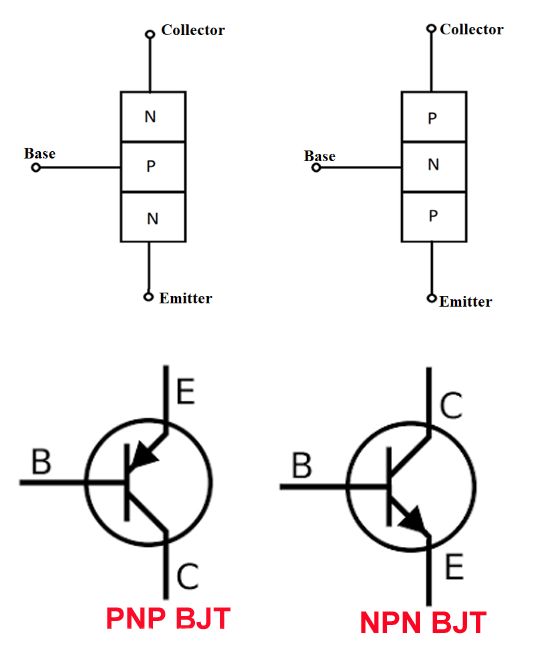
The difference in terms of circuits is that when connecting the power terminals, the emitter terminal of the PNP transistor is connected to the positive terminal, while for the NPN transistor, the positive terminal is connected to the collector terminal. From now on, this topic will be discussed based on NPN transistors only.
Case 1: When the base voltage is less than the emitter voltage, the flow of electrons from emitter to collector is blocked by the PN junction (this current is the current flowing from negative to positive terminal, while the conventional current is the current flowing from positive to negative terminal), because it is now in reverse biased state.
Case 2: When the base voltage is greater than the emitter voltage (Vb > 0.6v), the junction is reduced which allows current to flow from the emitter terminal to the collector terminal. Transistors must be operated in the saturation region because they provide low voltage drop in the saturation region.
Circuit Schematic
Given below is the NOT gate circuit using transistor. This circuit is designed and simulated using Proteus software.
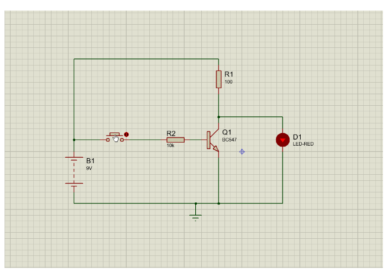
I set the supply voltage to 9V and I want to send 9mA to the led, so I use 100 ohms to limit the current. This same current must flow in the transistor I c = 9mA. The hfe of the transistor is 100, so the I b value should be 0.09mA. Since I b is 0.09mA, the base resistor value should be 10k ohms.
The following figure shows the current flow in both cases.
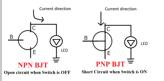
Case 1:
When the switch is in the off state, the current flowing to the base is zero and since these currents flow in the direction of the LED, the transistor acts as an open circuit and the LED starts to glow.
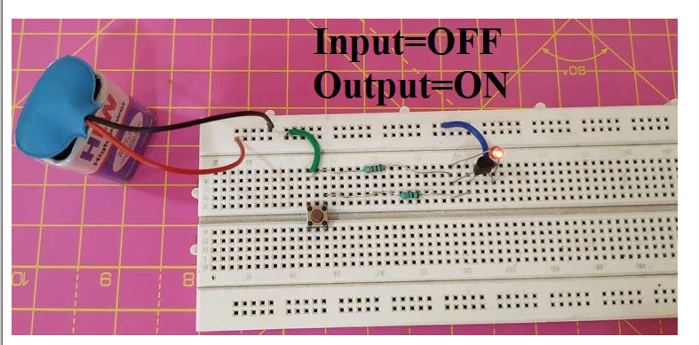
Case 2:
When the switch is in the on state, current starts flowing towards the base, which makes the transistor act as a short circuit, and as the current selects the lowest resistance, the resistance now offered by the transistor will flow in that path and the LED will be turned off.
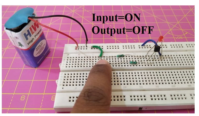
Hence, both cases have same input and output following the NOT gate truth table. Hence, we have built a NOT logic gate using transistors.
- What are the types of commonly used batteries?
- Advantages and disadvantages of organic semiconductors, the conductive mechanism of organic semiconductors
- How do you calculate the value of capacitors in series? Why use capacitors in series?
- Causes of PCB deformation How to prevent circuit board bending and warping
- Share a Motorola amplifier circuit
- Introduction of TDA4863J/4863AJ TV field scanning IC
- Using an Op Amp to Drive a Simple and Practical Power Amplifier
- Purpose and composition of amplifier circuit: low frequency voltage amplifier amplifier circuit
- Environmentally friendly and energy-saving LED AC/DC dual-purpose lamp
- Design circuit of voltage inverter using PWM
- Ultrasonic receiver circuit diagram for echo detection distance
- Transistor inverter circuit commonly used in radio medium wave band
- 90MHz transistor resonant power amplifier circuit
- superheterodyne radio circuit
- Transistor controlled rectifier circuit c
- Transistor controlled rectifier circuit b
- Picture tube final video driver amplifier
- buffer amplifier
- Ground drain amplifier circuit connections
- DC 12v converter working principle circuit diagram


 京公网安备 11010802033920号