Share a good fast charging protocol solution
Source: InternetPublisher:newlandmark Keywords: usb fast charging mobile power supply Updated: 2023/12/22
Many USB-powered consumer electronics devices have Qualcomm QC (Quick Charge) solutions built into them, allowing for fast charging at a different voltage than the usual 5.0 V. This gives the opportunity to use QC compatible power banks in projects that require more power or higher voltages such as 9/12 V.
The purpose of this project is to develop a device that can break the QC protocol and allow hobbyists, developers, engineers to use their power banks to provide more voltage/power for their next power-hungry project. Use this to draw 5 V and 9 and 12 V (up to 18 W) from any QC-compatible charger/power bank to power power-hungry items.
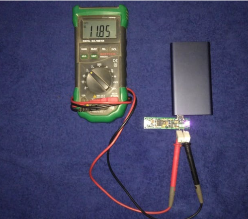
The image above shows the 5, 9, and 12 V outputs of the QC 2.0 compliant power supply, powering a 10 ohm 5 watt resistor.
Develop Hack Devices
The entire device is controlled by two active components - the LM1117 3.3V regulator and the ATtiny85MCU. All other parts are resistors, push button switches, connectors, jumpers, headers, terminals, prototyping boards, etc.
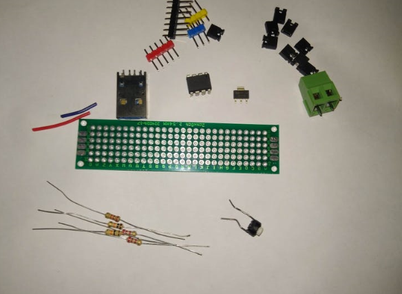
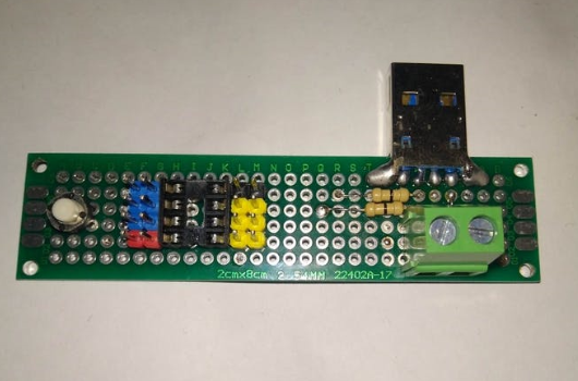
To build the device, the components are first placed in a neat layout and then soldered. Some short 0 ohm links are used to interconnect different parts.
There are jumpers to disable the onboard circuitry and enable programming. Because, the programming lines (SPI - MOSI, MISO, SCK) also act as GPIO during device operation.
Programming the ATtiny85 using ISP
Before programming the ATtiny85, remove it from the IC Base and place it on the breadboard. To program the ATtiny85, convert the Arduino UNO board into an ISP programmer by uploading "ArduinoISP" from File > Examples > ArduinoISP Sketch. This sketch is available in the Arduino IDE.
Programming the ATtiny85 requires the following steps:
Install ATtiny support for Arduino IDE (thanks to David A. Mellis)
Burning bootloader for ATtiny85 using Arduino UNO as ISP
Develop and upload code using Arduino UNO as ISP
The following circuit is ready to program the ATtiny85:
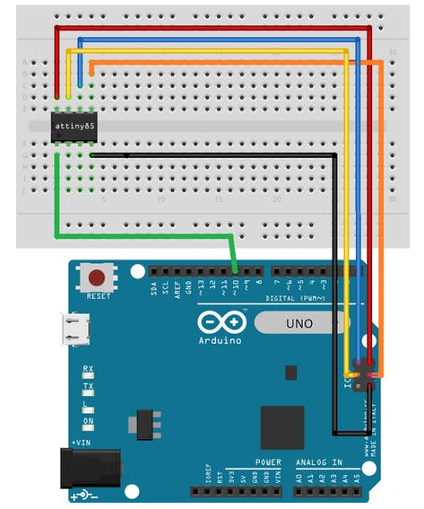
ISP = in system programmer
Alternatively, the ATtiny85 can be programmed to remain on the device by removing all jumpers around it.
Equipment operation
To use the device, you first need to connect it to a QC-compatible power bank (or charger). By default, the USB voltage of QC power bank is 5.0V.
All jumpers must be connected after uploading the code so that the MCU can communicate with the QC source via D+/-.
The LM1117 3.3 V regulator will start up and provide power to the ATtiny85. The MCU will start executing code. The 4 I/O pins of the ATtiny85 are connected to voltage divider resistors that will be used to output high and low levels. The other I/O pin is connected to a switch that will be initialized as an input pull-up. This switch takes user input to change the voltage of the QC source.
Now, before going into details, it's important to know how the output will change. Each type of USB (USB A, B, C, 1.1, 2.0, 3.0+) has at least 4 common lines/wires:
VBUS (default Vcc +5V)
D+
D-
ground
In a normal charger/power bank, VBUS is fixed because the power transfer is current limited, 500 mA, 1 A, 2 A produce 2.5 watts, 5 watts and 10 watts respectively.
But in the QC power supply device, there is an internal boost converter that can boost the voltage according to the requirements of the powered device (PD)! ! !
QC 2.0 (also known as 3.0) utilizes USB's D+ and D- to communicate with the PD. The PD sends voltage signals on D+ and D- and the QC charger will supply power accordingly by changing the VBUS voltage. Based on this CHY datasheet, here is a table explaining what signal pairs on D+/D- from the PD will cause the QC to provide what voltage output:
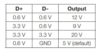
QC 2.0 supports startup when the voltage on D+ and D- is the same as the value in row 4 of this table for at least 1.25 seconds. If D+ goes to 0.0 volts (actually below 0.325 volts), QC support will stop and the output will be 5.0 volts. The output on VBUS can be changed by setting the voltage according to this table.
Here the 4 outputs of the ATtiny85 are connected to 2 voltage divider networks consisting of two 10k and two 2.2k resistors to generate these voltage signals for the D+/D- lines.
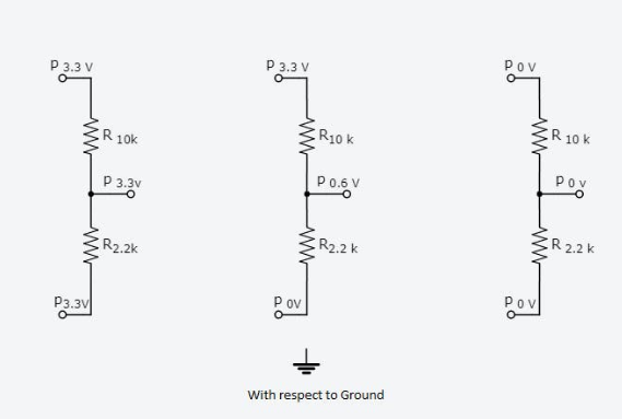
For example, to produce 3.3 V on D+, the top and bottom resistors connected to the two ATtiny85 output pins PB3 and PB4 would both be set high by code.
Likewise, to produce 0.6 V on D-, the top and bottom resistors connected to the other two ATtiny85 output pins (PB1 and PB3) will be set high and low respectively.
This way the QC 2.0 charger/power bank receives the voltage change request and changes accordingly. The Push Switch is configured to input PULLUP, and when not pressed, the MCU reads it high and code execution remains in a while loop, preventing any changes to the set voltage. When the user presses the Push Switch, the while loop breaks and sets the next voltage. Once again, code execution enters the next while loop to maintain the current VBUS voltage.
There is an LED that emits dim (5V), weak (9V), and bright (12V) light to provide the user with a visual representation of the output voltage.
Possible applications
Driving 12V LED strips
Powers longer range RF transmitters/receivers
Drive 12V relays, motors, etc.
Use an LM317 or LM2596 to get any voltage between 1.25 and 10 volts
9V infrared remote control driver
Robot car power supply
Laptop charging 20V
Any system up to 18W such as WiFI, LTE, S2E devices for IoT applications
Backup power for remote systems
Most LCD, LED monitors, printers, scanners
Low power portable computer
Support other QC classes
Since QC 2.0 Class B, QC 3.0 and QC 4.0 are backward compatible with QC 2.0 Class A, this device will likely work with all the latest chargers and power banks. But the voltage options will be 5.0, 9.0 and 12.0 volts. If other output voltages are required, read the CHY 100, 101, 103 datasheets and modify the code accordingly.
warn!
A high-quality QC power bank or charger with short-circuit protection must be used, and the external load must not exceed 18 watts. This can be ensured by checking the power rating label on the load equipment.
Outputting 20 volts must be avoided since the 1117 3v3 regulator can handle a maximum of 15 volts, this should be avoided from the MCU code by never allowing the D+ and D- lines to have 3.3 volts at the same time.
If a 20 Volt output is required (supported by QC 2.0 Class B and QC 3.0, QC 4.0), a voltage regulator capable of handling more than 20 Volts must be used (LM317 configured for 3.3 V). Otherwise both Regulator and MCU will be destroyed! ! ! !
Pay attention to the polarity of the output voltage, +ve is shown in red and -ve is shown by the thin blue line next to the output terminal.
Loose connections at USB male and female couplings must be avoided as they can generate heat due to contact resistance and reduce power supply efficiency.
During ISP programming, all jumpers must be removed to isolate the MOSI, MISO, SCK, VCC, GND, RESET pins from the rest of the circuitry on the board to avoid interfering with programming.
No code modifications should be made without a clear understanding of the QC charging protocol, this design is primarily for QC 2.0 (Class A) power supplies, but may be partially used for higher QC standards
Hack may not work with some QC chargers/power banks
GPIO switching must be done in the correct sequence to avoid terminating high voltage mode
Note: If the above points are not achieved, it is recommended not to copy this project, otherwise there may be a risk of fire hazard or equipment loss!
- A very convenient small power supply circuit to share
- Practical and convenient fax machine power supply control circuit
- MT3608 constitutes a 3.7V to 12V boost circuit diagram
- Op amp power supply decoupling bypass measures
- Visible laser digital control modulation driver
- Offline 8w LED Flyback Power Supply with PFC using NCP1014
- LED rechargeable flashlight circuit diagram
- Principles and precautions of active discharge circuit
- An ultra-low output voltage regulator
- Practical constant current charger-----Constant current charger
- Switching power supply circuit composition and detailed explanation of each part (1)
- Classic car battery charging circuit diagram
- Industrial product promotion and shopping guide DC power supply circuit
- Battery fast charging control integrated circuit design
- TBY-753A type fast charging regulated power supply circuit diagram
- 3-phase CPU power circuit using HIP6301 and HIP6601 chips
- 2-phase CPU power circuit using HIP6301 and HIP6601 chips
- One of the battery fast charging circuits
- Super Class A power amplifier power circuit
- New fast charging I simplified circuit


 京公网安备 11010802033920号