Important things to know about PCB routing and how to design the right routing for your PCB
Source: InternetPublisher:失踪的猫 Keywords: PCB design PCB routing Updated: 2025/01/03
Designing PCB has become very easy due to the loads of tools available. For beginners who are getting into PCB design,
He may not care much about the trace characteristics used in the PCB. However, as you climb up the ladder, it is very important to pay attention to PCB traces. In this article, we have compiled some important things you should know about PCB traces and how to get the right traces for your PCB design.
Trace width and thickness:
As you probably know, in PCB, the copper wire that connects two points on the PCB is called a trace. The copper trace has a specific width, which we call the trace width, and a specific height or thickness. The thickness is determined by the PCB manufacturing company standards. You usually choose the copper weight in the quote,
It depends on your project requirements when you order PCB. It is measured in ounces, usually the copper thickness of PCB is 1oz. This means that when 1
It is the thickness produced when ounces of copper are flattened and evenly distributed over a one square foot area.
Tracking Type:
Generally, there are two types of tracks in PCB. They are –
Signal trace
Power routing
Signal traces are traces that carry data signals, and power traces carry the current that powers the circuit.
Power routing:
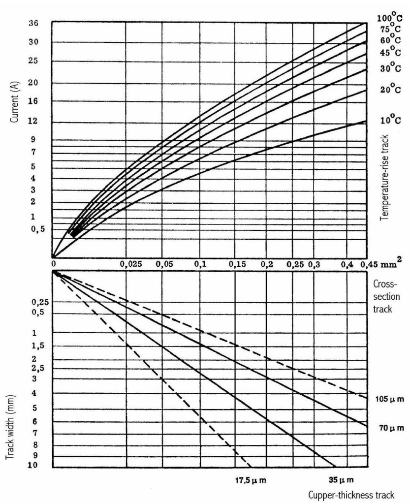
For power lines, sufficient trace width is required to ensure that the required amount of current can be safely transmitted without damaging the board. The relationship between trace width and current carrying capacity in a PCB is very simple. The cross-sectional area of the trace and the temperature rise determine the current carrying capacity of the PCB. The cross-sectional area of the trace is proportional to the copper thickness and the trace width.
Temperature rise:
This is a key factor that indicates the expected temperature rise that can be expected when the PCB is operating. This is usually affected by factors such as resistance, voltage drop, maximum current, etc. There are other factors that affect this such as trace length, number of vias, pads, and components, etc. It is always a good practice to reduce high voltage drops, which can also reduce power losses in the design to control temperature rise. The higher the temperature rise, the higher the PCB trace width.
Current carrying capacity:
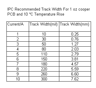
Higher currents require higher trace widths. The IPC standards for conductor thickness and width for a common 1 oz/sq ft PCB are shown below. However,
Due to tolerances and variations in PCB processes, it is always recommended to use larger values.

The following figure shows the recommended trace width relative to current at a 10C temperature rise.

Note that track width increases as current increases. Also, if you need to calculate trace width for a specific current and other custom factors, there are several online tools that can be used to calculate the trace width required to carry a given current while keeping the trace temperature below a specified limit. Actual results may vary depending on the application and conditions. You can visit one of these websites to make the calculations as needed.
Signal trace:
Signal traces or data lines make things more complicated, especially when you are working on high-speed circuits. In such cases, factors such as signal integrity and trace impedance need to be considered.
Signal Integrity:
In simple terms, signal integrity is the tendency of an electronic signal to retain its initial characteristics while passing through a medium. A signal received with the same amplitude, phase, frequency, power, and waveform as when it left its source has high signal integrity. In reality, this does not exist. Instead, we use some design techniques to keep signal integrity at an optimal level. This article introduces signal integrity and design considerations that help achieve high signal integrity in your designs.
Trace impedance:
This property applies to high-speed designs. For high-frequency signals, PCB traces do not behave like simple connections. Each trace in a PCB design has some series inductance that is often overlooked in low-speed designs, but in high-speed designs, this inductance can increase and affect the performance of the board. In addition, each signal trace maintains some capacitance value between the trace and the return path. If not checked, these factors can degrade the performance of the PCB because the impedance at different points in the PCB will be different.
This requires a method called controlled impedance in PCB design, where designers should try to keep impedance constant at every point in the circuit. This article details trace impedance and the design considerations for designing a controlled impedance PCB.
- What is a D flip-flop and how does it work?
- What is power factor and three ways to improve it
- Beautiful crown wreath made with LED
- Important things to know about PCB routing and how to design the right routing for your PCB
- Touch circuit design and analysis
- Purpose and composition of amplifier circuit: low frequency voltage amplifier amplifier circuit
- FL52C4 induction electronic greeter
- How to make a four-level water level indicator with full water alarm function
- Homemade Simple Frequency Synthesis Signal Source
- A night light made of LED
- Impedance control of through holes in PCB design and its impact on signal integrity
- Do you understand the anti-static ESD function in PCB design?
- Do you know PCB design tips to improve the electromagnetic compatibility of circuit boards?
- What software is needed for PCB design?
- PCB schematic diagram reverse derivation step method
- 555 square wave oscillation circuit
- 555 photo exposure timer circuit diagram
- Introducing the CD4013 washing machine timer circuit diagram
- Simple level conversion circuit diagram
- 555 electronic guide speaker circuit diagram for blind people


 京公网安备 11010802033920号