|
The OP
Published on 2022-1-23 20:36
Only look at the author
This post is from RF/Wirelessly
| ||
|
Personal signature
射频【放大器】 |
||
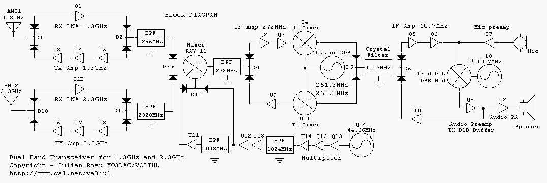
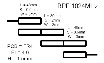
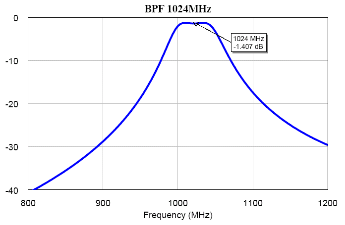
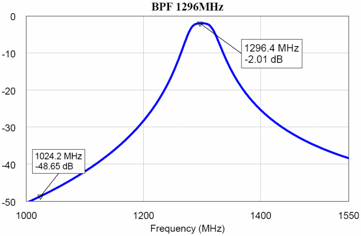
- 【Posts】Dual-band transceiver for 1.3GHz and 2.3GHz bands
- 【Posts】Is it feasible to use the low-cost feature of 433MHZ frequency band wireless control to replace Bluetooth devices?
- 【Posts】Compact grounded asymmetric coplanar strip-fed flexible multi-band reconfigurable antenna for wireless applications
- 【Posts】[nRF7002-DK Wi-Fi 6 Development Kit Review] 2.4/5G HZ dual-band, WiFi networking capability test
- 【Posts】[Analysis of the topic of the college electronic competition] - 2016 Shanghai TI Cup B "Design of short-wave frequency digital communication system"
- 【Posts】Please recommend a cheap RF transmitter with variable frequency of 415M~475M and price <10 yuan
- 【Posts】Will there be conflicts between Wi-Fi and Bluetooth in the same frequency band?
- 【Posts】US NB frequency band
- 【Download】Freescale MC13202: Second-generation 2.4 GHz transceiver for wireless sensing and control applications
- 【Download】ADF7023: High-efficiency, low-power ISM-band transceiver IC
- 【Download】IA4421 Universal ISM Band FSK Transceiver 38 pages 2.9M.pdf
- 【Download】ADF7023 High Performance, Low Power ISM Band Transceiver IC
- 【Download】2.4G band PCB antenna design
- 【Download】PCB antennas for each frequency band, directly available
- 【Download】Global operator 2G/3G/4G frequency band list
- 【Download】Design and implementation of multi-band signal source based on ADF4350
- 【Design】10.5GHz (X-band) patch antenna
- 【Design】ELRS dual-band tuner
- 【Design】Low noise amplifier evaluation board using the BGU7003 matched to the 868 MHz ISM band
- 【Design】# Fifth Lichuang Electronic Design Competition# Multi-band QRP shortwave radio station based on GD32
- 【Design】OM17057: Demonstration board for BGU6104 low noise amplifier, ISM and LTE bands
- 【Design】PSC9131RF13-0113: 13dBm LTE/3G RF card, Bands 1 and 13
- 【Circuits】Build a 5-band graphic equalizer circuit using NE5532 and LM833
- 【Circuits】Production of 900MHz frequency band directional antenna
- 【Circuits】Wideband Wien bridge oscillator circuit diagram
- 【Circuits】High power HF band standing wave meter/power meter
- 【Circuits】U-band 4 data signal wireless transmission circuit (PT2262)
- 【Circuits】Fast full-band phase-locked loop circuit diagram
- 【Articles】Mouser now sells Semtech LoRa? LR1121 multi-band transceiver
- 【Articles】China is the first in the world to allocate the 6GHz frequency band for 5G/6G systems
- 【Articles】The Ministry of Industry and Information Technology officially plans to use the 76-79 GHz frequency band for automotive radar
- 【Articles】Zhuoshengwei: Launches RF discrete devices and module products suitable for 5G NR frequency band
- 【Articles】Filter components for noise and intermodulation testing in 4G LTE bands
- 【Articles】Design of a power divider suitable for ISM dual-band
-
Application suggestions for 2.1GHz and 3.5GHz frequency bands in 5G networks
summary:Withthecontinuousdevelopmentofmobilecommunicationnetworks,operatorshavedifferentfrequencybandresources,includinghigh,mediumandlowfrequencybandsHowtoreasonablyandefficientlyutilizespectrumresourcesistheprimaryissuethatoperatorscurren ...
-
Can the 2.4GHz and 5GHz frequency bands supported by CC3135MOD work online at the same time?
Canthe2
-
I was deducted money for the wrong picture
IdrewadiagramwithamicrocontrollerinitIsimplyremovedtheDCDCandreplaceditwithanLDOtostartitnormallyAftertheleaderknewaboutit,hedeductedtheperformance
- OPEN SCOFIELD WINTER WARDROBE
- Newbie Report Newbie Report
- [ACM32F070 supporting capacitive touch development board to evaluate the basic functions of UART serial port]
- Choosing the right GaN power amplifier - the design is so simple
- The Perseverance rover landed on Mars. Let’s talk about how demanding space is on equipment.
- Infineon Angle Sensor Application Unlocking Machine See how many you can find? Good gifts are waiting for you!
- FPGA experience talk (Xi'an Datang Telecom).pdf
EEWorld Datasheet Technical Support
-
Qualcomm launches its first RISC-V architecture programmable connectivity module QCC74xM, supporting Wi-Fi 6 and other protocols
On November 14, Qualcomm announced the launch of two connectivity modules, QCC74xM and QCC730M, f
-
It is reported that memory manufacturers are considering using flux-free bonding for HBM4 to further reduce the gap between layers
On November 14, according to Korean media ETNews, Samsung Electronics, SK Hynix, and Micron are a
-
ON Semiconductor CEO Appears at Munich Electronica Show and Launches Treo Platform
During Electronica, ON Semiconductor CEO Hassane El-Khoury was interviewed by Power Electronics N
- AMD launches second-generation Versal Premium series: FPGA industry's first to support CXL 3.1 and PCIe Gen 6
- SEMI: Global silicon wafer shipment area increased by 6.8% year-on-year and 5.9% month-on-month in 2024Q3
- TSMC's 5nm and 3nm supply reaches "100% utilization" showing its dominance in the market
- LG Display successfully develops world's first stretchable display that can be expanded by 50%
- Seizing the Opportunities in the Chinese Application Market: NI's Challenges and Answers
- New diaphragm-free solid-state lithium battery technology is launched: the distance between the positive and negative electrodes is less than 0.000001 meters
- Photoresist giant JSR Korea EUV MOR photoresist production base started construction, expected to be put into production in 2026
- Problems with STM32 and passive buzzer playing sound
- Embedded Tutorial_DSP Technology_DSP Experiment Box Operation Tutorial: 2-28 Building a Lightweight WEB Server Experiment
- OPA847IDBVR op amp domestic replacement
- AG32VF407 Test UART
- [Digi-Key Follow Me Issue 2] Chapter 1: Sharing on receiving the goods
- What model is this infrared receiver? Which model can be used instead? Thank you
- Selling brand new unopened ZYNQ 7Z020 FPGA core board
- The LORA module used in the lithium battery-powered water meter setting can save energy when 100 water meters are installed in one corridor.
- I would like to ask, when a port is set to RX0, is it necessary to set the input and output direction of this port?
- Why is this year so difficult? It’s even more difficult than during the pandemic. I’m 30 and facing unemployment. I’m so confused.
- Ask about the voltage regulator test question
- [Xiaohua HC32F448 Review] About Xiaohua Semiconductor's UART interrupt sending and PRINTF construction and redirection
- 【BIGTREETECH PI development board】 HDMI output test
- 【BIGTREETECH PI development board】+08. Audio test (zmj)
- [Xiaohua HC32F448 Review] +RTC electronic clock
- # STM32H7S78-DK Development Kit Three-week Review: Implementation and Analysis of Simple Sound Collection and Storage Using SD Card Reading and Writing
- [STM32H7R/S] Review⑧ nano edge ai studio training a model--Part 1
- [2024 DigiKey Creative Competition] A "fortune-telling" artifact based on Raspberry Pi
- New energy vehicle on-board AC slow charging and maintenance
- Embedded Engineer AI Challenge Camp (Advanced): Deploy InsightFace algorithm on RV1106 for real-time face recognition of multiple people
- I want to make a self-driving car. I saw one on Bilibili that costs 300 yuan. I am hesitant.
- [K230 Embedded AI Development Board Review] + License Plate Recognition and Billing Management
- How to deploy LVGL free graphics library on low-cost ARM platform, based on Allwinner T113-i
- Please help me analyze the reasons why EMI fails.
- ChatTTS is really awesome!




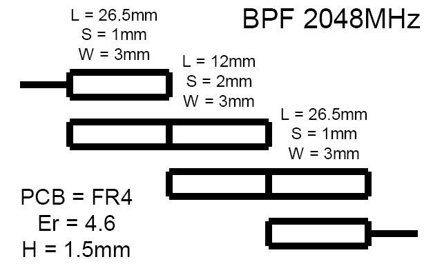
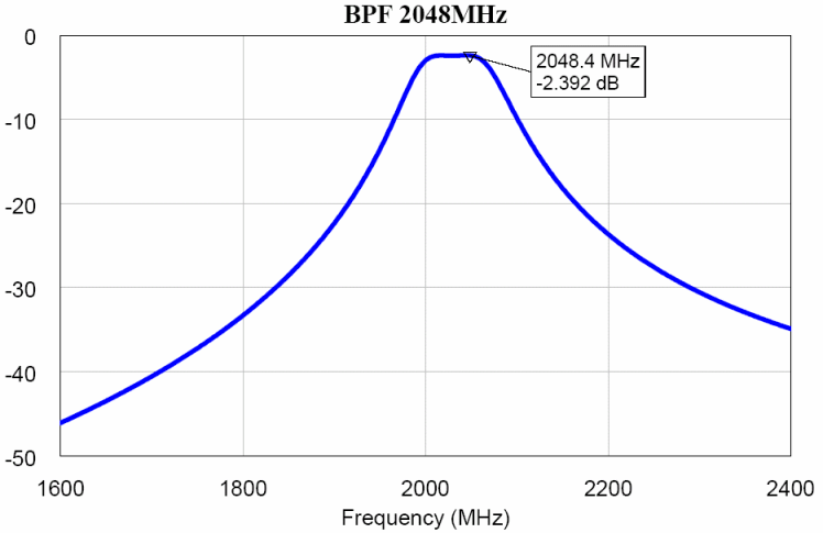
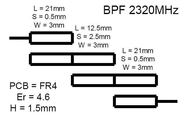
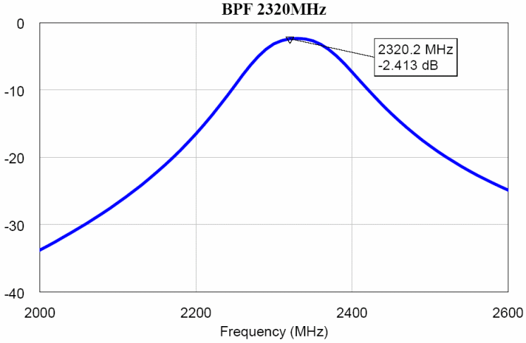
 提升卡
提升卡 变色卡
变色卡 千斤顶
千斤顶